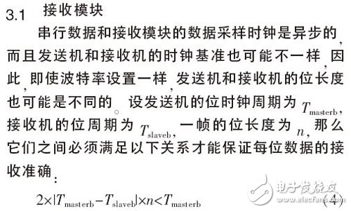
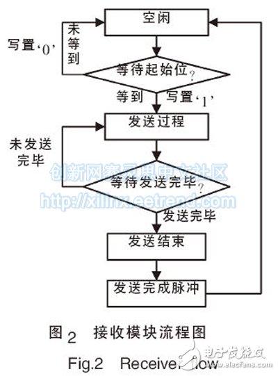
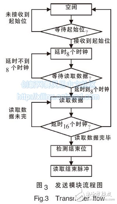
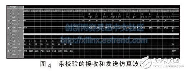
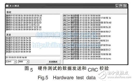
Abstract: Cyclic Redundancy Check (CRC) is often used in communication based on Serial Asynchronous Receiver Transmitter (UART). Common CRC check circuits are mostly serial check, and the clock cycles required for verification are more. A parallel algorithm for table or input matrix conversion requires storing a remainder table and consuming a large amount of hardware resources. This paper successfully uses the logic relationship between the input and check polynomials to successfully apply the byte-based parallel CRC check algorithm to the UART controller and verify it through Xilinx's programmable gate array (FPGA) chip. Multiple byte checksums. It takes 1/8 clock cycle to verify a bit, which reduces the clock frequency required for verification, improves communication efficiency, and ensures communication reliability. UART is widely used in industrial communication control. In the communication process, it is often necessary to add a CRC check code at the end of the data to ensure the reliability of data transmission. CRC check code is an effective but very simple coding technology. Due to its high probability of detection and easy hardware implementation, it is widely used in mobile communication, computer, USB and other fields. The traditional hardware implementation is serial shift. The bit mode verifies each bit received in turn, and it takes 8 clock cycles to verify each bit. The parallel algorithm of CRC check has a lookup table method and some methods derived based on the lookup table method, but these methods all need to store a CRC remainder table with a large length, and the performance is low. Directly using the logical relationship between the input byte data and the polynomial, the logical expression of the CRC is derived, and the method is straightforward and concise [2]. The parallel byte CRC check mechanism is introduced into the UART-based data communication, which implements a byte-based CRC parallel check, which requires 1/8 clock cycles for each bit. This solution has been successfully used in acquisition and monitoring systems. The CRC parallel algorithm is derived from the LFSR (Linear Feedback Shift Register). The basic principles are as follows: Again, the circuit form is determined and the CRC polynomial is converted to a circuit transfer diagram form [3] according to the LFSR (Linear Feedback Shift Register). As shown in Figure 1. Finally, the input data is substituted, and each bit is introduced into the register, and each bit in the data is sequentially introduced to the input end of the LFSR, and finally the logical expression of each bit in the CRC result after all bit inputs is obtained, namely: expression. Asynchronous communication has the following characteristics: The transmission format of the character frame enables the sender to insert different time intervals between characters according to the application requirements, that is, the transmission of each character is random, which is the main feature of asynchronous communication [4]. The start of each character transmission is always based on a start bit, and then the receiver is synchronized with the sender (unified format). The communication parties can change the communication protocol at any time according to the needs of the application, that is, change the data bit, the parity bit, the stop bit length, and the data transmission rate. In the data stream of asynchronous communication, one character is regarded as an independent information unit, and the relative time when characters appear in the data stream is arbitrary. The receiving end does not know in advance. Once each character is sent, both the transmitting and receiving parties pre- A fixed clock rate is transmitted to each bit. Therefore, for asynchronous communication, the character format and baud rate must be unified before the CPU communicates with the peripherals. It can be seen from the above equation that the establishment and hold time of the clock in the FPGA chip and the interference caused by the transmission process are not considered. When n is constant, the baud rate is higher, the bit period error is smaller, and the accumulated error is smaller, and the data transmission is performed. The smaller the error rate. Rxd (input pin) changes from '1' to '0' to represent the start bit. In order to eliminate the glitch interference, 16 oversampling methods are generally used to ensure that each bit of data is correctly received, and each bit of data is The intermediate sampling is used as the sampling result to minimize the cumulative error of subsequent data bit detection. Therefore, when counting to the center of the start bit of the flag, data is collected every 16 acquisition cycles until all data bits are acquired, and the stop bit is finally detected, and then the reception completion flag pulse is output. The software flow chart is shown in Figure 2. The clock frequency of the sending module is the baud rate clock period. The transmitting module does not need to consider the clock error problem. It only needs to send each bit according to the sending period. In order to make the transmitter send one byte each time, the rising edge trigger is used to start sending. The task is automatically stopped after one frame is sent. Therefore, when the rising edge of the transmit enable pin is detected, the start bit, data bit, and stop bit are sequentially output in the transmit clock drive. The software control process is shown in Figure 3. The read/write control module is two independent control modules, but in the system is a half-duplex mode, that is, when the command frame is received, the data is sent according to the protocol content, and the two module processes communicate with each other through the signal mechanism, and the trans_over is set. For the status signal sent, receive_over is the accepted status signal, and the receiving module is in the working state first. When receiving one frame of data, receive_over is set to '1' and waits for the transmitting module to complete trans_over after the transmission module is completed. The transmitting module first trans_over Set '0', wait for receive_over to set '1', send trans_over to '1' after sending the data and wait for receive_over to be set to '0'. Through these two signals, the work of the transmitting and receiving modules is coordinated. The experiment uses Xilinx's XC3S400 as the FPGA chip. The experimental data and function simulation waveforms are shown in Figure 4. The serial port baud rate is 9600, 8bits data bits, no parity bit, and 1 stop bit. Start bit, stop bit does not participate in CRC check. In order to keep in line with the CRC-16 check of most of the upper layer protocol software versions in practice, the input data is inverted first, and the value of the register is set to '1' when reset; the CRC byte participates in the check when receiving, and the judgment is made. The result is 0x0000 to determine if the data transfer is correct. When transmitting, the lower 8 bits of the CRC are transmitted first, and then the upper 8 bits are transmitted. In the process of transmission, the CRC result is also involved in the verification. After the data is sent, the lower 8 bits of the CRC result are directly sent twice, and the high 8 bits and the lower 8 bits are automatically exchanged. The program is downloaded to the FPGA chip for testing, and the UART communication experiment is performed by using the PC-side serial port control software. Some of the data is shown in Figure 5. The core board of the hardware circuit is XC3S400 (TQ144 package), and the serial port chip adopts Max3232. The basic protocol is that if the received data check correctly returns the corresponding byte length data, in this example 0x01, 0x03 is the frame header, 0x00, 0x01 is The address, 0x00, 0x06 is the data length. After repeated experiments, the transceiver system maintains very high transmission reliability. Flag pulse delay output: When receiving one byte of data is completed, if the data latch and the flag pulse are synchronized, then the first check byte is the CRC-16 module input data when idle, so in order to maintain each time The verification is the data received this time. The positive pulse of the CRC check completion flag should be slightly delayed, so that the data is updated first, and the check pulse is followed, which ensures the continuous byte data input of the CRC-16 module. The test is correct. In this paper, the pulsed delay output is realized by passing the positive pulse of the flag through a D flip-flop. It can be seen from Fig. 4 and Fig. 5 that the simulation results are the same as the measured results, indicating that the UART controller based on the parallel CRC algorithm implemented by FPGA has the correct data transmission and achieves the design goal. The serial CRC circuit requires more clock cycles when performing more data transmission. The CRC parallel algorithm can effectively reduce the clock frequency of the check. This paper applies the parallel CRC algorithm to the UART communication, which reduces the need for verification. The clock cycle ensures the reliability of data transmission, has achieved good results, and has important practical value. At present, it has been applied to multi-channel high-voltage data acquisition and monitoring instruments in the laboratory, and the work is stable and reliable. Explosion Proof Motor,Explosion Proof Servo Motor,Exproof Motors,Explosion Proof Ac Motor Yizheng Beide Material Co., Ltd. , https://www.beidevendor.com