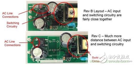
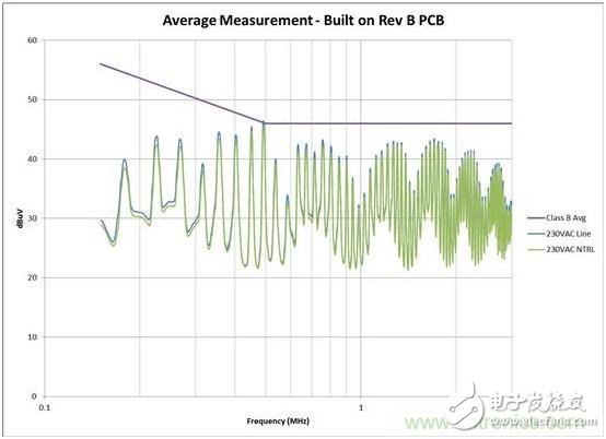
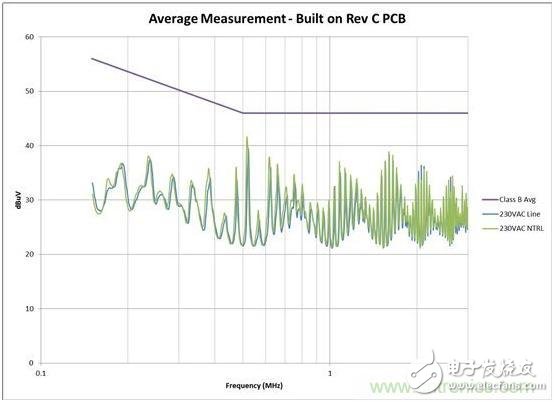
Electromagnetic interference EMI The interference signals generated by electronic equipment are transmitted through wires or common power lines, and mutual interference is called conducted interference. Conducted interference has caused confusion for many electronic engineers. How to solve conducted interference? Here, we will focus on what happens when parasitic capacitance is directly coupled to the power input wires. 1. A few fF of stray capacitance will cause the EMI scan to fail. Essentially, switching power supplies have nodes that provide high dV/dt. The mixing of parasitic capacitance with high dV/dt creates EMI problems. When the other end of the parasitic capacitor is connected to the power input, a small amount of current is pumped directly to the power line. 2. View the parasitic capacitance in the power supply. We all remember in the physics class that the capacitance between two conductors is proportional to the surface area of ​​the conductor and inversely proportional to the distance between the two. Look at each node in the circuit and pay special attention to nodes with high dV/dt. Think about the surface area of ​​the node in the circuit layout and how far the node is from the input line of the board. The drain and snubber circuits of the switching MOSFET are common culprit. 3. There are tips for reducing the surface area. Try to use a surface mount package whenever possible. FETs in the upright TO-220 package have an extremely large drain tab surface area, but unfortunately it usually happens to be the node with the highest dV/dt. Try replacing it with a surface mount DPAK or D2PAK FET. By placing a primary ground plane on the low-level PCB under the DPAK tab, the bottom of the FET is well shielded, significantly reducing parasitic capacitance. Sometimes the surface area needs to be used for heat dissipation. If you must use a TO-220 type FET with a heat sink, try connecting the heat sink to the primary ground (instead of grounding). This not only helps to shield the FET, but it also helps to reduce stray capacitance. 4. Let the switch node and the input connection pull apart. See the design example in Figure 1, where I ignored this simple principle. Figure 1. Getting the input wiring too close to a node with a high dV/dt increases the conducted EMI. I reduced the noise by about 6dB by simply adjusting the board (no circuit changes). See the measurement results in Figures 2 and 3. In some cases, close to high dV/dt for input line wiring can even damage common mode coils (CMC). Figure 2. EMI scan from board layout where the AC input is closer to the switch circuit Figure 3. EMI scan from board layout with large distance between AC input and switching circuitry Have you ever experienced an EMI improvement with little or no improvement after significantly enhancing the input filter? This is most likely because some stray capacitance from a high dV/dt node is directly coupled to the input line. Effectively bypass your CMC. To detect this, temporarily short the windings of the CMC on the PCB and connect a secondary CMC in series with the input wires of the board. If there is a significant improvement, you will need to re-layout the board and pay special attention to the layout and routing of the input connections. Now let's look at the most common source of common mode EMI problems: power transformers. This problem is caused by the parasitic capacitance between the primary winding and the secondary winding and the high dV/dt of the primary winding. This capacitor between the windings acts as a charge pump, causing stray current to flow to the secondary side that is typically connected to ground. Here are four common tips to minimize this problem. 1. Perform a primary winding so that the highest dV/dt appears on the outer layer. The voltage potential varies with each number of turns. For example, in a flyback topology, the maximum voltage swing appears at the end that connects the drain of the FET (see Figure 1). Keeping the "silent" layer close to the nearest secondary layer minimizes the dV/dt that occurs across the inter-winding capacitance. With this technique, it should be clear that the external winding may have become a problematic source of noise that may couple to other targets near the transformer. A shield winding may be required around the outer winding. 2. Use a shield winding between the primary winding and the secondary winding. Inserting a single-layer winding with one end connected to the input or input return allows the stray current to exit the secondary winding and return to the source. The cost of this technology is a slight increase in the design complexity of the transformer and increased leakage inductance. 3. Use a "Y capacitor" between grounding and secondary grounding. The capacitor provides a lower impedance path back to ground for stray current. This local path in the power supply prevents these currents from finding another path back to the source via ground. However, there are certain safety restrictions on how much capacitor can be used. 4. Add a common mode coil. Sometimes other techniques mentioned are not sufficient to reduce EMI below the required level. Adding a common mode coil not only increases the common mode impedance, but is also very effective in reducing conducted noise. But this will result in additional component costs. When selecting a common mode coil, pay attention to checking the impedance curve with respect to frequency. In some cases, all coils will become capacitive due to their own inter-winding capacitance problems. USB charger, USB Adaptor, Charging USB Ports, USB quick charger NINGBO COWELL ELECTRONICS & TECHNOLOGY CO., LTD , https://www.cowellsocket.com

