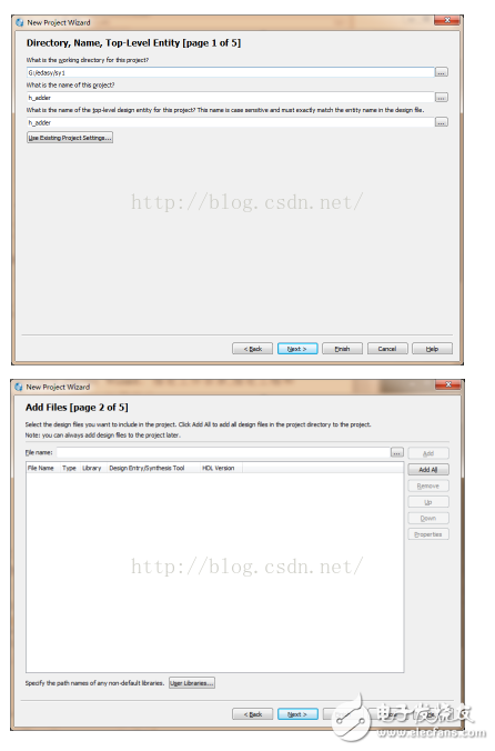
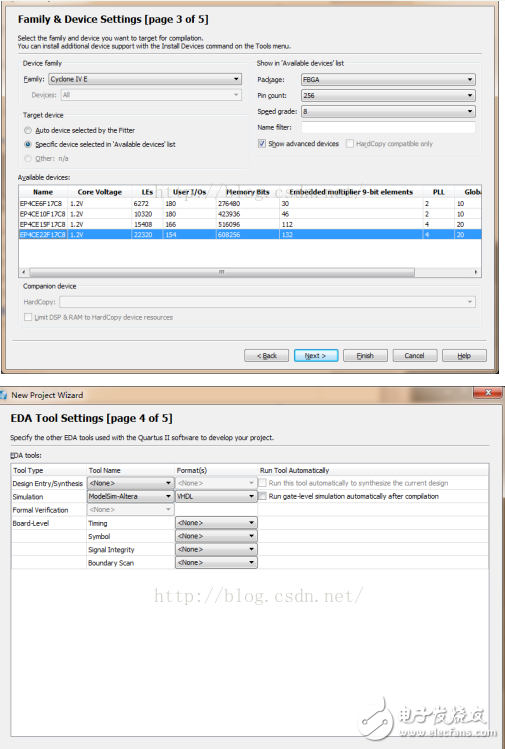
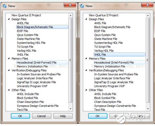
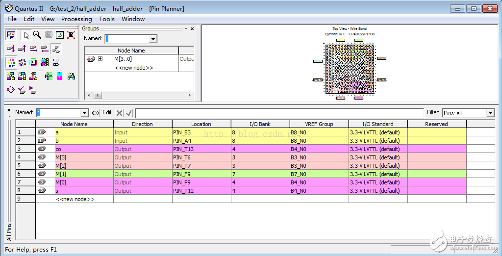
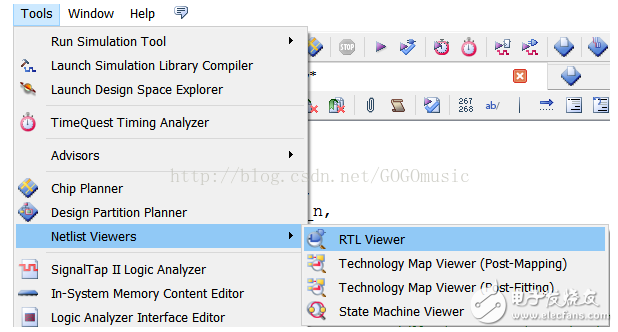
Take the QuartusII13.0EDA software as an example to introduce the EDA design flow of Verilog text input. 1. First create a new folder on the D drive or G drive, etc., and name it with English letters, for example, create a folder SY1. FPGA project directory: dev: project is built in this folder, project settings Core: IP core storage area Src: user code save area Sim:testbench simulation test file Doc: Design Reference Document Then open the Quartus II software, select File / New Project Wizard, specify the working directory, specify the project and the top design entity; note: the working directory name can not have Chinese. As shown in Figure 4-3. Figure 4-3 New project Figure 4-4 Adding a design file 2. Add a design file. Add the design file to the project. Click "Next". If there are already created files such as Verilog, you can select the path in File name and add it, or select Add All to add all the design files that can be added (.VHDL, .Verilog schematic, etc.). If you don't click "Next" directly, you can add it after you have established the project. We will not add it here, as shown in Figure 4-4. 3. Select the FPGA device. The EP4CE22F17C8 devices are selected as follows: (Family selects CycloneIVE, Available device selects EP4CE22F17C8, Packge selects FBGA, PinCount selects 256, Speedgrade selects 8); EP3C80F484C8 devices are selected as follows: (Family selects CycloneIII, Available device selects EP3C80F484C8, Packge selects FBGA, PinCount selects 484 Speedgrade chooses 8); I have used both of them so far. As shown in Figure 4-5, click "Next". Figure 4-5 Selecting a device Figure 4-6 Selecting an emulator 4. Select an external synthesizer, emulator, and timing analyzer. The Quartus II software supports external tools. The Quartus II software version 9.1 or later does not have its own simulation tool. When simulaTIon selects Modelsim-Altera, Format:Verilog, it uses Modelsim simulation, as shown in Figure 4-6. After the selection is complete, click Next. ". Click “Next†to pop up the “Project Settings Statistics†window, which lists the related settings of the project. Finally click "Finish" to end the project settings. 5. Create a new schematic/text file. If you do not add a design file when you build the project, you will need to create a new file. Click "file" and click "new" to select. If you select the schematic input, select BlockDiaqram/SchemaTIc File, as shown in Figure 4-7. If you choose Verilog text input, select Verilog HDL File, as shown in Figure 4-8. Figure 4-7 Creating a new schematic file Figure 4-7 Creating a new VHDL text file 6. Click on "Save" and the schematic or Verilog text file will be added to the project. 7. Verilog text design. When designing the text, enter the corresponding Verilog program and save it. Pay special attention to the file name saved and the name of the top-level file module. 8. Compile. Click Processing/StartCompilaTIon to compile. If the compilation is wrong, re-check and modify the schematic or Verilog program, save and compile again, prompt the compilation is successful, start pin lock and download. Figure 4-13 Pin Lock 10. Pin Lock Method 1: Pin Lock Information As shown in Figure 4-13, select Assignments/PinPlanner to lock the pins and lock all the I/O pins. Pin Lock Method 2: See the next blog documentation. 11. After the pin lock is completed, global compilation (including synthesis, adaptation) is performed again, and clicking Processing/StartCompilaTIon. 12. Global compilation is complete, check if there is a compilation error under the software. View the integrated RTL view method as shown in the figure: 13. Download to the EDA lab platform. Download can choose JTAG mode and AS mode (JTAG download mode to download files directly into the FPGA, AS download mode to download files to the configuration chip, so you can power down storage). Select Tool/Programmer, select JTAG download mode, select Add File, add .sof file (AS download selects .pof file) and select Program/Configure. Click “Start†to start downloading. When using the download for the first time, first click "HardwareSetup..", open the Hardware Setup dialog box, then click Add Hardware, select usbblaster and click "Select Hardware", select the download form as usb blaster. 14. Unassigned pins must be tri-stated when doing Quartus II projects. Quartus II --" Assignments --" Device...-- Device -- " Device & PinOptions... -- " Unused Pins -- " Reserve all unusedpins : AS input tri-stated. Failure to set the unassigned pin to a three-state input may result in damage to the main or peripheral chip.
Application: Automobile Wire Harness
Gauge: AWG 28 to AWG 16
Length: Customized
We can provide first price for products produced in our factory; for sourcing products,we can also provide most competitive price because we have
large relationship among our friend factory.
Automotive Wiring Harness,Auto Wiring Harness,Universal Automotive Wiring Harness,Effect Assurance Cable Wire Harness Dongguan YAC Electric Co,. LTD. , https://www.yacentercns.com

Place of Origin: Dongguan, China (Mainland)
Connector: Molex, JST, TYCO, AMP, JAM, KET,Amphenol, Wago,Weidmuller, Phoenix,
Wires & Cables: UL, VDE standards
Inspection: 100% inspection before delivery
Certification UL, IATF16949, CE