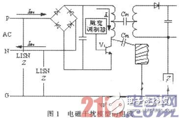
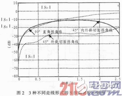
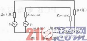
Abstract : PCB circuit design is very important in production and life. This paper starts from the issue of electromagnetic compatibility, discusses PCB circuit design, and electromagnetic interference in the design of PCB circuit. Analyze the setup and routing of single-wire, multi-conductor lines and components to derive some design specifications and skills for wiring in PCB circuits. If these principles and specifications are used in the initial stage of circuit design, the electromagnetic interference problem existing in the wiring will be quickly solved by the PCB circuit designer. The so-called PCB (Printed Circuit Board) is actually a printed circuit board. It is a relatively important electronic product and is a provider of electrical connection of electronic components. It plays a major role in the connection between circuit components and electrical components. The role. It is a support body for electronic components and plays a supporting role for circuit components and devices. The strength of anti-jamming capability is directly affected by the excellent design of printed circuit boards. Therefore, the arrangement and anti-interference ability of the circuit must be taken into consideration by the designer when designing the circuit. PCB printed circuit boards can be classified into single-plane, double-plane, and multilayer boards depending on the number of circuit layers. Common multi-layer boards are generally 4-layer boards or 6-layer boards, and complex multi-layer boards can reach more than 10 layers. Although many years of design and practice, electronic engineering personnel have summarized some norms and design experiences. However, as of now, the country does not have clear requirements and rules in this regard. Based on this, in practice, we can only make full use of design principles and related rules in the design of circuits, and conduct overall planning and design, especially the anti-jamming design of the circuit. By doing so, we can effectively avoid serious electromagnetic interference problems in the circuit design practice, but also effectively reduce the frequency and save the design cost, which is very important for effectively reducing the time of the electrical circuit design. 1 Composition of Electromagnetic Environment in Printed Circuit Boards Electromagnetic interference sources, coupling paths and receivers constitute a simple electromagnetic interference model, as shown in Figure 1. Microprocessors, microcontrollers, electrostatic discharges, transmitters, and instantaneous power actuators are common sources of interference and appear at higher frequencies in printed circuit boards. The clock circuit is usually the largest broadband noise generator in a micro-control system. Conduction coupling and radiation coupling together constitute a coupling approach and play an important role in printed circuit boards. With different coupling approaches, the resulting interference problems are naturally different. For example: 1) The mutual inductance occurs frequently in the wire, and the capacitance may increase greatly when in a partial state; 2) Printed circuit wire crosstalk; 3) High frequency signal generated when a high frequency signal is printed on the wire Electromagnetic field; 4) Electromagnetic radiation interference due to the clock signal; 5) Reflection interference; 6) Interference due to a series of improper operations. In short, many objects are likely to become sensitive components, including electronic components and wires. If you want to grasp the overall layout of the board and the position of components and components, you need to work hard on the cabling. Only reasonable cabling and achieving electromagnetic compatibility standards are the best way to achieve this goal. 2 Single traces on a printed circuit board PCB circuit design, the differential trace coupling is small, only accounts for 10 to 20% of the coupling degree, more is the coupling to the ground. When the local plane is discontinuous. Without a reference plane area, differential trace coupling provides a return path. PCB routing is required to avoid the appearance of right angle traces. The right-angle traces have a negative effect on the signal, so the traces in the PCB generally have a 45-degree corner or a circular-arc corner line. The differences between right-angle and non-right-angle wires are as follows: 1) The corner can be equivalent to the capacitive load on the transmission line and reduce the rise time; 2) The corner can also resist the signal reflection caused by the inconsistency; 3) Electromagnetic Interference may occur due to the right angle tip. Different corner lines have obvious differences in angle. Figure 2 uses an FDTD numerical method to perform the experiment. The simulation compares the reflection transmission characteristics with the reflection characteristics. The corner line reflection and transmission performance of the 45 degree outer mitre is better than the other two corner lines. These three types of traces are worse than arc corners, but the radians are more expensive to characterize. This is because the engraving of the arc requires exquisite plate making technology. Exquisite technology will inevitably lead to an increase in cost, so it is usually the case that when you choose to route, you will be stuck on the corner line of the 45-degree oblique chamfer. 3 Analysis of Crosstalk of Multi-conductor Transmission Lines in Application The frequency of the transmission signal and the operating frequency of the machine must pay attention to the principle of moderateness in the PCB circuit design. If the megahertz level is reached, the interference to the line is very serious. The main cause of interference between traces is crosstalk. During the PCB electrical circuit design process, crosstalk should be properly taken care of to minimize the occurrence of crosstalk problems. In practice, it can be seen that if crosstalk occurs, there are usually at least 3 conductors and two lines carrying signals. As shown in Figure 3, the third conductor is only for reference. In practice, it can be seen that the interaction between the source and the victim circuit usually produces a VS. Under this action, zs and zL will generate inductive voltages and currents. The zs and the source are interconnected, and the zL is mainly related to the load. interconnected. In order to reduce the occurrence of interference, the author proposes the following suggestions and design plans: 1) Logical devices with functions as the main basis to control the bus structure; 2) Minimizing the physical distance of components; 3) Strictly controlling the length of wiring traces 4) The components should not only be far away from the I/O interface, but also avoid data interference as much as possible; 5) ensure the accuracy of the impedance-controlled trace path, and usually the traces with larger frequency-wave energy should be considered; 6) Provide some intersecting traces to ensure proper distances between traces to ensure minimum inductive coupling; 7) The wiring layers next to each other should be vertical, which can reduce the capacitive coupling between layers; 8) Strengthen The spacing and distance control between the signal and the ground; 9) The wiring layers must be separated and must be routed along the same axis to ensure that the wiring layers are separated into pre-solid plane structures. 4 Distribution of traces inside the printed circuit board Under normal circumstances, functional units and equipment meet the requirements of electromagnetic compatibility, mainly determined by the degree to which the basic components of the circuit meet electromagnetic characteristics. When selecting an electromagnetic component, electromagnetic characteristics and circuit assembly are two factors that must be considered, otherwise the selected electromagnetic component is inferior. This is mainly because the element response characteristics away from the fundamental frequency determine whether electromagnetic compatibility is achieved. In most cases, the degree of coupling between the external response (such as the length of the lead) and the component is determined by the circuit assembly. Need to pay attention to the following points. PCB size is one of the first factors to be considered. The PCB size should be moderate, too large or too small. If it is too much, there will be a lot of lines when printing, in order to increase the impedance and reduce the anti-noise performance, but its cost will increase; if it is too small, it will lack the ability to dissipate heat and the affected object will expand to the phase. Neighboring lines. Based on this, before determining the location of a particular component, the actual size and dimensions of the PCB should be adequately measured; based on the circuit's capabilities, all components in the circuit are planned and adjusted. In the actual operation, in order to be able to To greatly reduce the loss of high-frequency component lines, reduce the complexity of parameter distribution, and avoid electromagnetic interference, it is necessary to think of ways to separate, so that there is a distance between the input and output components. Reduce the high potential difference between components or wires to avoid short circuit due to discharge. In the process of circuit debugging, if the component has a high voltage, it should be placed in a position that is not easily encountered. At the same time, we must also pay attention to the effective fixation with a bracket, if soldering more than 159 components. The relatively large, heavy heat components cannot be adapted to the printed circuit board and should be eliminated. This component should be configured on the chassis floor. The thermal problem should be taken into account when installing. The thermal element cannot be near the heating element. The structural requirements of the complete machine should be considered first, especially when layout adjustable components such as potentiometers, switches, etc. If it is an internal adjustment, it should be placed in an area that is easy to adjust, such as on the top of the printed board; if it is off-board adjustment, you need to consider the adjustment knob. The required area for the PCB positioning holes and fixing brackets must be released first. The distribution of all components of the circuit must be based on its functional units. Therefore, the following points must be made: 1) In order to make the signals more circulated, the circuit flow must be considered. Each functional circuit unit must be placed in a reasonable position. In the area, this can also maximize the signal in a uniform direction; 2) In the layout, it is necessary to closely surround the core element of each functional circuit. When components are arranged, they should pay attention to the principles of symmetry, no clutter and closeness. The number of wires used to connect the various components should be minimized. 3) When the circuit is operating under high load conditions, the actual distribution needs to be considered. To maximize the parallel distribution of components in the circuit. Parallel distribution can make the external appearance look better, facilitate welding, and also help a lot of production; 4) The components on the edge of the circuit board can not exceed 2 mm from the center of the circuit board; for the circuit board It is recommended to design it as a rectangle. The length is 1.5 times the width, or 1.3 times. 5 Common EMC Design Software Electromagnetic radiation at the interface between the PCB board and the outside is a factor to be considered during analysis. In addition, consider the electromagnetic radiation of the power layer in the PCB board and the radiation problem of the high-power wiring network. Nowadays, board-level and system-level interconnection simulations have been extensively applied in the design of EMC software, both of which are mainly based on Cadence's technology. At the same time, SI/PUEMI simulation analysis was also applied. Germany's INCASES company invented EMC-WORKBENCH, which has an important driving force in EMC simulation analysis. As a result, INCASES has become a leader in the industry and has made significant contributions to EMC's progress. EMC-WORKBENCH helps designers, especially in the technical difficulties of electromagnetic compatibility. At the same time, the design process was changed, the workload was reduced, and some design procedures were deleted. Thanks to the application of EMC simulation technology, PCB design has quickly entered a new era. In particular, electronic engineering personnel can use this technology to achieve short-term high-quality, high-reliability designs. In the process of implementing EMC simulation analysis, it will inevitably bring greater opportunities and broader development space for the development of circuit design and PCB manufacturing industry. In practice, it can be seen that a circuit board may come from a large number of manufacturers, and there is a big difference in their functionality. Designers need to fully understand the characteristics of the components when they analyze the EMC, so that the Perform specific simulation operations on it. If this operation is viewed from a traditional perspective, it seems to be a very arduous project. However, the emergence of IBIS SPICE has played a very significant role in the analysis of EMC issues. 6 Conclusion In short, in the actual PCB design process, we must strictly follow the relevant design specifications, to comply with the principles and requirements of anti-jamming design, and only in this way can the electronic circuit be in the best performance state. At the initial stage of PCB design, comprehensive consideration must be given to the problems in the wiring, so as to effectively reduce the design cycle and improve the design quality. Profibus cable connectors are used to support various BUS systems . The Connection Cable is designed for fixed indoor installation or occasional outdoor installation in the industrial networks. The signal wires are generally provided in the form twisted pairs. Applications: industrial automation, machinery equipment, Sensors & actors, automation process and robotic machines and field-bus system. RoHS, REACH compliant. Custom Profibus,Profibus M12 B-Code Connector,Female Mould Cable Connector,4 Pin Male Connector Kunshan SVL Electric Co.,Ltd , https://www.svlelectric.com

