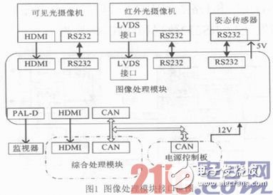
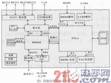
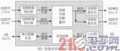
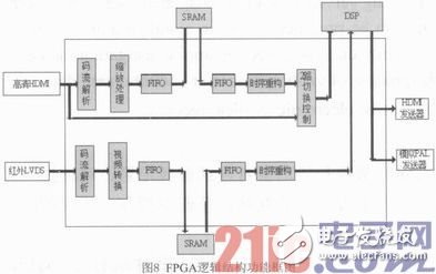
Abstract: This paper introduces an image processing scheme based on DM648 and FPGA architecture, expounds the composition principle and structure of image processing module, and introduces the internal circuit design of the module and the internal image processing logic of FPGA. The text processing module designed by Muwen can support algorithm processing such as cutting, scaling, superimposing and switching of high-definition video images. With the advent of the digital age, video image processing is becoming more and more important as an important part of digitalization. In particular, the processing technology of high-definition video has become a research hotspot in the industry. This paper proposes a video image processing hardware solution that supports multiple video input and output interfaces for the characteristics of video processing technology. The image processing module designed in this paper is mainly used to collect the image information of the target, and after processing by image cutting, scaling, superposition and switching, the image data is sent to the system integrated processing module through the HDMI interface, through the CAN bus interface and RS232. The interface controls peripherals and obtains status information for peripherals. The main specific functions of the image processing module are as follows: receiving visible light video information of a high-definition camera, the video input interface is an HDMI interface; receiving infrared video information of the infrared camera, the video input interface is an LVDS interface; receiving an attitude sensor, a white light camera, and the RS232 communication interface Information such as infrared cameras and other peripherals; image processing of visible light video or infrared video information, and output through HDMI and PAL-D interfaces; receiving control commands sent by the system main control board through the CAN interface. Image processing module interface application block diagram shown in Figure 1. Through analysis, the main function of the image processing module is to perform multi-channel video processing, and the amount of processed video data is large, and the real-time image requirements are high. Therefore, the implementation of the image processing module adopts DSP (DM648)+FPGA. The DSP is used to implement complex video processing algorithms. The use of FPGA ensures image delay and is also beneficial to the expansion of system functions. The system block diagram of the image processing module is shown in Figure 2. In addition to the core circuit of DSP+FPGA, the module includes HDMI, LVDS decoding circuit, HDMI, PAL-D encoding circuit, single-chip control circuit, CAN Ethernet and other interface circuits. The image processing module mainly completes the sampling, switching and transmission functions of the video signal, and simultaneously completes the communication function through the CAN bus interface and the RS232 interface. The information flow of the image processing module is shown in Figure 3. The digital HDMI video signal of the visible light camera and the digital grayscale video signal of the infrared camera are received, and the video data is preprocessed, and then sent to the video cutting, switching and superimposition processing. The unit, the processed video data enters the video data sending unit and is sent out through one analog PAL-D interface and one digital HDMI interface. One analog PAL-D interface and one digital HDMI interface display the same content. Receive and send 4 R$232 data and 1 CAN data. The visible light camera HDMI video decoding circuit completes the decoding of one HDMI input video, and sends the YCrCb signal conforming to the high definition format to the FPGA after decoding, and other video processing functions are implemented by the FPGA. The visible light camera HDMI video decoding circuit diagram shown in Figure 4, using a single ADV7441 to complete the video decoding function. The infrared camera LVDS video decoding circuit completes the decoding of one LVDS input video, and sends the decoded YCrCb signal to the FPGA, and other video processing functions are implemented by the FPGA. Infrared camera LVDS video decoding circuit diagram shown in Figure 5, using a piece of NaTIonal Semiconductor's DS90CR286AMTD to complete the video decoding function. The HDMI video transmission circuit completes the transmission of one HDMI video, sends the YCrCb signal after the FPGA to the HDMI transmission chip, and encodes the parallel digital video into a serial differential TMDS physical link signal. The HDMI video transmission circuit diagram is shown in Figure 6. The ADV7513 of AD is used to complete the encoding and transmitting function of digital video. The PAL-D video transmission circuit completes the transmission of one analog PAL-D video, and sends the YCrCb signal after the FPGA to the PAL-D transmission chip to encode the parallel digital video into a composite analog PAL-D video signal. The PAL-D video transmission circuit diagram is shown in Figure 7. The GM7121 of Guoteng Company is used to complete the encoding and transmitting function of digital video. Because the image processing module has to complete some complex image processing algorithms, the performance requirements of the image processor are relatively high. The DSP processor of this design selects the DM648 processor, and the DM648 is a high developed by TI for image processing applications. Performance low-power processor, which integrates 5 configurable video input and output ports and image co-processors. The processor clocks up to 1.1GHz. The FPGA chip selects the XC6SLX100 from XILINX's SPARTAN-6 series. FPGA has the advantages of large capacity, high performance, low power consumption and low cost, and has a wide range of applications in graphic image processing. The image processing module mainly performs image preprocessing functions such as format conversion, cutting, scaling, and superposition of video through FPGA, and completes complex algorithm functions such as video enhancement, recognition, and splicing through DM648. As shown in Figure 2, after the video enters the module, it first decodes, then enters the FPGA for pre-processing. After the FPGA processing is completed, it enters the DM648 through the video port, and completes the image processing function of the complex algorithm in the DM648. After the processing is completed, it passes through the video port. Output to the FPGA, complete the video format conversion and other functions in the FPGA for encoding output. The processing logic inside the FPGA will be highlighted below. The functional block diagram of the FPGA logic structure is shown in Figure 8. The image signal timing of the visible video camera digital video decoding is a YbitCb signal conforming to the high-definition standard 16-bit color depth. The image signal timing after decoding the digital video of the infrared camera is based on the PAL-D timing, but the pixel is reduced from 768 to 384 in the whole line. The visible and infrared video data is stored in the SRAM after being buffered by the FIFO, and then preprocessed, cut, fused, and switched in the FPGA, and then sent to the video interface of the DM648, and the DM648 performs user-specified algorithm processing on the received image data. After that, the video timing control logic outputs to the HDMI video transmitter and the PAL-D transmitter. The visible light camera HD HDMI video is 1920 & TImes; 1080P/25FPS, 16-bit data signal, clock frequency 74.25MHz, data rate is 1.118Gbps, its video buffer SRAM bus data bit 32 bits, clock up to 167MHz, the project design working frequency is 74.25 MHz, the data rate is 2.376Gbps, which is twice the data rate of the HMDI interface, which can meet the requirements of video read and write cache. The infrared camera's video is finally converted into a 1-way PAL video, which can meet its cache requirements with a single SRAM. The image processing module based on DM648+FPGA architecture has the advantages of two kinds of signal processing chips, which effectively improves the complexity and speed of video processing, enhances video processing performance, and has stable and mature technology, small module size and low power consumption. Etc. In the subsequent research, the DM648-based image processing algorithm will be deeply researched to improve the performance of the algorithm and further improve the video processing capability of the module.
Innosilicon Asic Miner:Innosilicon A9 ZMaster,Innosilicon A9++ ZMaster,Innosilicon A9+ ZMaster
Innosilicon is a worldwide one-stop provider of high-speed mixed signal IPs and ASIC customization with leading market shares in Asian-Pacific market for 10 consecutive years. Its IP has enabled billions of SoC's to enter mass production, covering nodes from 180nm to 5nm across the world`s foundries including: GlobalFoundries, TSMC, Samsung, SMIC, UMC and others. Backed by its 14 years of technical expertise in developing cutting-edge IPs and ASIC products, Innosilicon has assisted our valued partners including AMD, Microchip and Microsoft to name but a few, in realizing their product goals.
Innosilicon team is fully devoted to providing the world's most advanced IP and ASIC technologies, and has achieved stellar results. In 2018, Innosilicon was the first in the world to reach mass production of the performance-leading GDDR6 interface in our cryptographic GPU product. In 2019, Innosilicon announced the availability of the HDMI v2.1 IP supporting 4K/8K displays as well as our 32Gbps SerDes PHY. In 2020, we launched the INNOLINK Chiplet which allows massive amounts of low-latency data to pass seamlessly between smaller chips as if they were all on the same bus. With a wide range of performance leading IP in multiple FinFET processes and 22nm planar processes all entering mass production, Innosilicon's remarkable innovation capabilities have been proven in fields such as: high-performance computing, high-bandwidth memory, encrypted computing, AI cloud computing, and low-power IoT.
innosilicon zec miner,Innosilicon A9 ZMaster,innosilicon a9 50ksol miner,innosilicon a9 miner,a9 50ksol zmaster Shenzhen YLHM Technology Co., Ltd. , https://www.asicminer-ylhm.com


