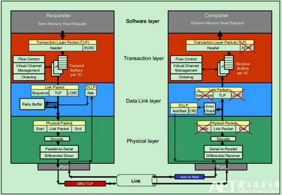
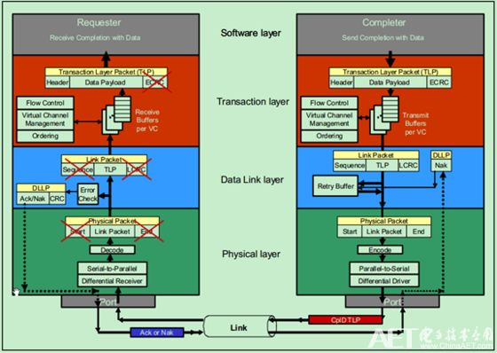
The previous series of articles briefly introduced the PCIe bus architecture, transaction layer, data link layer, and physical layer. Below we use a simple example to review and summarize. As shown in the figure below, the Requester application layer (software layer) first sends the following information to its transaction layer: 32-bit (or 64-bit) Memory address, transaction type, data amount (in DW), TC (Traffic Class, ie priority), Byte Enable and Attributes. Then the receiver's transaction layer uses this information to create a Mrd TLP (Memory Read transaction layer packet) and writes the Requester's ID (BDF, Bus & Device & Function) into the header of the TLP so that the Completer can use this The BDF returns Completion information to the Requester. Then the TLP will be put into the corresponding VC Buffer according to the value of its TC, and the Flow Control logic will check whether the corresponding receiving VC Buffer space of the receiving end of the vehicle is sufficient. Once the VC buffer on the receiver is adequate, the TLP is ready to be sent to the receiver. Note: There are actually two types of TLP headers. The 32-bit address corresponds to the 3DW header, and the 64-bit address corresponds to the 4DW header. This will be described in detail in subsequent articles. When the TLP reaches the Data Link Layer, the data link layer adds a 12-bit Sequence Number and a 32-bit LCRC. The TLP (ie DLLP) after adding this information will make a backup in the Replay Buffer and then send it to the physical layer. After receiving the DLLP, the physical layer adds Start Characters (Frame Characters), and then performs Strip Byte, Scramble, and 8b/10b encoding in order. It is serialized and then sent to the physical layer of the adjacent PCIe device. After the physical layer of the receiving end PCIe device (ie, the complete device) receives the data, the operations opposite to the sending end are sequentially performed. It recovers the clock from the data and sends the recovered DLLP to the data link layer. Completer's data link layer first checks the LCRC in the DLLP. If there is an error, it sends a Nak type DLLP to the Requester. The DLLP contains the Sequence Number in the DLLP it receives. After receiving the Nak DLLP from the Completer, the Requester's data link layer finds the Sequence Number and finds the corresponding DLLP in the Replay Buffer based on the sequence number, and then resends it to the Completer. If the data link layer of the Completer does not detect LCRC errors, it also sends an Ack type DLLP to the Requester, which also contains the sequence number in the DLLP it receives. After the Requester's data link layer receives one of the Ack DLLPs, it will find a backup of the corresponding DLLP in the Replay Buffer according to the sequence number, and discard it (Discard). When the data link layer of the receiving PCIe pen (ie, Complete) receives correctly the DLLP (including the TLP) from the Requester, it is further sent to the transaction layer, and the transaction layer checks the ECRC (optional), and The TLP is parsed and then the parsed information is sent to the application layer (software layer). As shown in the figure below, the application layer of the Completer will perform corresponding processing according to the received information. After the processing is completed, the data will be sent to the transaction layer. The transaction layer will create a new TLP based on this information (ie, CplD, Completion with data). . According to the BDF information in the previously received TLP, the original Requester is found, and then the CplD is sent to the Requester. This sending process is basically the same as the process that the Requester sends the TLP (Mrd Request) to the Completer. So this is not repeated here. Note: If the Completer is unable to return valid data to the Requester, or if it encounters an error, it will return CplD instead of Cpl (Completion without data). After the Requester receives CLP's TLP, it will know that an error has occurred. The application layer (software layer) performs the corresponding processing.
Product Name: Car Charger
Place of Origin: Guangdong, China (Mainland)
Brand Name: OEM
Output Type: DC
Connection: Other
Rated Voltage: 12V-24V
Working Temp: 0-55℃
Weight: 36g
Materials: PC+ABS
Color: White Black
Warranty: 1 year
Suitable for:Most digital devices
SMART PROTECTION & ATTRACTIVE DESIGN ------ Intelligent circuit design protects against short circuiting,over-heating,over-current,and over-charging. Charging stops when battery is full. Car charger with blue LED indicator,which makes it convenient to find exactly where the connection should go; And the light is soft enough not to distract at night. Dual USB Car Charger Adapter,USB Smart Port Charger ,Car Charger,USB Car Charger For Phone Shenzhen Waweis Technology Co., Ltd. , https://www.waweispowerasdapter.com
