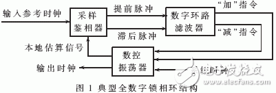
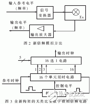
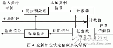
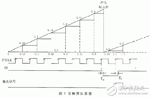
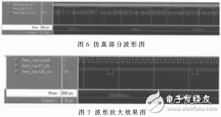
With the advent of the digital age, more and more fields use integrated circuits to design circuits, and EDA designs such as FPGA/CPLD are more accepted by hardware engineers. Its modular design brings a lot of convenience to designers and saves system development time. Designers only need to call these modules or IP cores, and then combine them to achieve a simple function. The all-digital phase-locked loop (DPLL) is a typical example. However, DPLL has many defects in application, such as long phase lock time and narrow capture band. In order to avoid these shortcomings, this article designs a brand-new phase tracking frequency multiplication system, which effectively improves these indexes of DPLL, and has been well applied in the project. The so-called all-digital phase-locked loop means that all the loop components are digitized, and the phase-locked loop is composed of a digital phase detector (DPD), a digital loop filter (DLF), and a digitally controlled oscillator (DCO). The structure of a typical all-digital phase-locked loop is shown in Figure 1. The phase detector it uses is a lead-lag digital phase detector. The phase detector obtains the information that the phase of the input clock is ahead or lagging behind the local estimated clock phase in each cycle, so that the phase error output of the phase detector has only two states: lead or lag. After the lead or lag information of the error phase is sent to the sequence filter, an "plus" or "minus" pulse control command to the DCO is generated to change the clock period of the DCO, so that the phase of the local estimated clock is close to the phase of the input clock. The loop filter uses a K counter. Its function is to count the phase error sequence, that is, filter, and output the corresponding carry pulse or borrow pulse to adjust the phase of the output signal of the I/D numerically controlled oscillator, so as to achieve phase control and lock. However, there is a pair of contradictions between phase lock time and phase jitter. A large value of K is beneficial to suppress noise. Because of a large value of K, the counter cannot fully account for a small amount of noise interference, so there will be no carry or borrow pulse Output. But this way the capture band will become smaller, and it will increase the time for the loop to enter the locked state. On the contrary, if the value of K is small, it can speed up the lock-in of the loop, but the K counter will frequently generate carry or borrow pulses, which will cause phase jitter, increase synchronization error, and correspondingly reduce noise suppression. . Therefore, it is very important to select an appropriate K value for a general DPLL. For frequency multiplication circuits, most of them are currently developed based on phase-locked loop technology, so the contradictions in the phase-locked loop design will inevitably be brought into the frequency multiplication design. Even if the frequency multiplication range of the system is wide, the disadvantages of poor spectral purity, obvious jitter, and large noise due to the PLL's own defects are inevitable. In recent years, more and more scientific research institutions have devoted themselves to the development of new phase-locked frequency multiplication systems, which have made new breakthroughs in both digital and analog fields. In terms of simulation, Fordahl has developed a new doubling simulation method as shown in Figure 2. This method works well in high and low frequency bands, and at the same time effectively improves the defects in the phase-locked loop design. In terms of digital, a completely new structured incomparable all-digital phase-locked frequency multiplication circuit has been successfully developed by a scientific research institution and has been put into use. Its structure is shown in Figure 3. The design is completely based on FPGA/CPLD design and development, with short phase lock time (only one system clock cycle tpd delay), and at the same time has the advantages of incomparable circuit, no jitter, no internal oscillator, and low power consumption. This article combines the above two methods and designs a new phase-locked frequency multiplication system based on the operating thought of FPGA pipeline. While having the advantages of the above two frequency multiplier circuits, it also enhances the accuracy of frequency multiplication and expands the range of frequency multiplication. Within the range allowed by system resources, the relationship between chip area and speed can be reasonably utilized, with fewer logic units, Design a high-speed frequency multiplication system. This new phase-locked frequency multiplication system consists of four modules: synchronization preprocessing module, counter module, algorithm module, and selection output module. Its structure is shown in Figure 4. 3.1 Principle First, synchronize the input reference clock (CLK_IN) and copy the input signal so that the input signal is synchronized with the global clock (SYSCLK) (even if there is an error between the copied signal and the input reference clock, the error is less than one SYSCLK cycle) , And then count CLK_IN based on SYSCLK. If the signal CLK_IN jitter is very small or the period is constant, count in units of n (n》1) cycles; if the jitter is large (generally related to external environment and physical factors), count in units of one cycle, and Pass the count value as input to the algorithm module. The algorithm module gets an enable signal (/EN) after a series of algorithm processes. Finally, use the characteristics of the setup time (Tsu) and the hold time (Th) to select the output of the SYSCLK with the enable signal /EN low to obtain the required frequency multiplication signal. Starting from the principle of PLL frequency multiplication, the frequency of the input reference clock after multiplication cannot be greater than the system clock frequency, so the problem of multiplication of the input clock is ultimately the problem of frequency division of the system clock. After the system clock is divided, it is output as a signal on the one hand and as a feedback signal on the other. After the frequency is divided by N (multiplier value), the local estimated signal is obtained, which passes through the DPLL loop to make it in phase with the reference clock, so that the in-phase N-multiplied output signal with the input reference clock is obtained. It can be seen from here that the DPLL-based frequency multiplication circuit performs phase lock and clock multiplication simultaneously. Therefore, the frequency multiplication process is bound to be restricted by DPLL's own factors. In the frequency doubling system designed in this paper, the system synchronization process and the frequency doubling process are two independent processes, and there is no dependency relationship between them, so the two processes can be optimized separately. (1) The phase lock problem. It can be considered as a "synchronization" problem. The most important concept in the synchronization process is the "frame of reference". For the phase-locked loop, the local estimation signal is calculated based on the input reference clock; and if the system clock is used as a reference, the local copy signal must be The clock is synchronized and in phase with the input reference clock. The advantage of this is that the phase lock is fast and the chip system speed (frequency) is improved. (2) Frequency multiplication problem. Since the local replicated clock is synchronized with the system clock, and all signals synchronized with the system clock must be synchronized with the replicated signal, the frequency multiplication of the local replicated signal can be simplified to the frequency division of the system clock. For example, assuming that the frequency of the input reference signal is 64kHz and the frequency of the system clock is 64MHz, it is now required to design a circuit whose output signal is in phase with the input reference signal and the frequency is a 9.6MHz clock. Through calculation, the output signal is 1500 times of the input reference signal, which is divided by 20/3 of the system clock frequency. Therefore, as long as the 20/3 frequency divider circuit is designed, the output signal can be a multiplier signal that is 1,500 times the input reference clock. The algorithm idea is shown in Figure 5. 3.2 Algorithm SYSCLK is used as the system clock of the accumulator. The bit width of the accumulator is determined according to the precision of frequency division. The accumulation operation is valid on the rising edge of the system clock, and the initial value of the accumulator is 0. Because it is divided by 20/3, the accumulator increases by 0.15 at the rising edge of the clock, and at the same time judges the magnitude of 0.15 and 1. Since 0.15<1, /EN=1. When the second rising edge of the clock arrives, after the accumulated 0.15 is equal to 0.3, the size of 0.3 and 1 is judged at the same time, since 0.3<1, /EN=1. By analogy, the value of the accumulator should be 1.05 when the seventh rising edge of the clock arrives. Since 1.05》1, /EN=0. Then take the difference of 1.05 minus 1, 0.05 as the initial value of the accumulator for the next calculation, and proceed in order to get the /EN signal. In FPGA design, the rising edge of the clock is generally used. According to the FPGA setup time Tsu and hold time Th, although the rising edge of SYSCLK cannot be taken during the setup time, the eighth edge can be taken during the hold time. Rising edges. In this way, an output signal with a frequency of 9.6MHz can be obtained. 4.1 Phase lock time Because this design is based on the system clock, the maximum phase error between the local copy signal and the input reference signal is one SYSCLK cycle. This design uses Altera's Cyclone series EP1C3T144-8 chip, and the system clock frequency can reach up to 105.65MHz. Therefore, the maximum error is 9.465ns. If optimized again, it can reach within 7ns. 4.2 Frequency multiplication range and accuracy This design uses an arbitrary number frequency division algorithm, and the frequency range of the output signal after frequency multiplication can be from 0 Hz to the highest frequency of the system clock. Therefore, for accuracy, any value after the decimal point can be achieved, but the deliberate pursuit of accuracy is based on the premise of wasting chip area. The selected accuracy value shown is also determined according to the number of logic units of the chip. Part of the simulated waveform is shown in Figure 6, and the enlarged effect diagram is shown in Figure 7. The new phase-locked frequency doubling system proposed in this paper has been applied in the project and tested in practice. The performance fully meets the expected requirements and the effect is good. Energy Storage System,Solar Energy Storage System,2Mw Energy Storage System,Lifepo4 Energy Storage System Jiangsu Stark New Energy Co.,Ltd , https://www.stark-newenergy.com