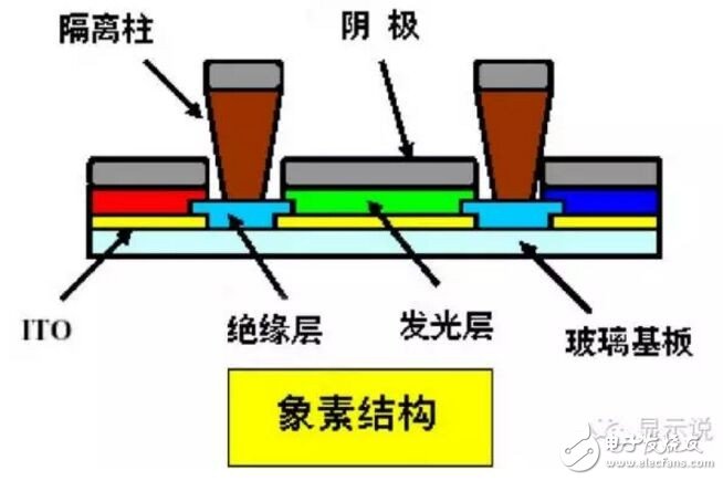
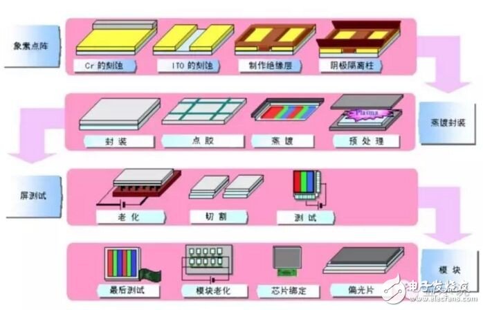
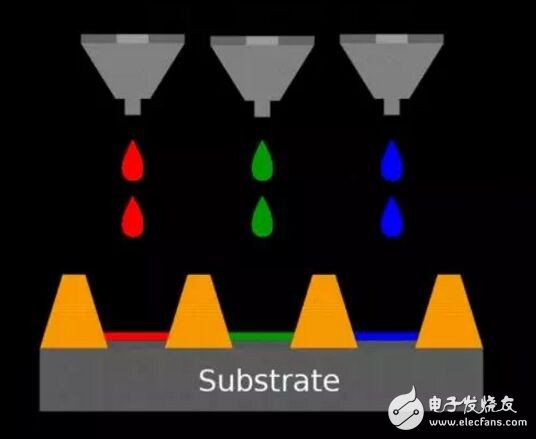
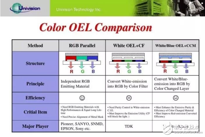
First of all, to understand the evaporation technology, this has to start from the structure of OLED. As shown in the figure below, the typical structure is to make a layer of tens of nanometers thick luminescent material on the ITO glass. The ITO transparent electrode and the metal electrode respectively add voltage as the anode and cathode electrodes of the device, and drive electrons and holes under a certain voltage. Injection from the cathode and the anode to the electron and hole transport layers, respectively, electrons and holes migrate to the light-emitting layer through the electron and hole transport layers, respectively, and recombine in the light-emitting layer to form excitons and excite the light-emitting molecules, the latter The visible light is emitted by radiation relaxation. Radiation light can be observed from the ITO side, and the metal electrode film also functions as a reflective layer. OLED structure schematic Of course, the structure is also much more complicated when it comes to the entire panel, including isolation columns, insulation layers, and the like between sub-pixels. AMOLED also has a TFT backplane that controls each pixel switch. OLED pixel structure diagram In simple terms, evaporation is the process of heating, electron beam bombardment heating and laser heating in a vacuum to evaporate the vaporized material into atoms or molecules, which then move linearly in a large free path, colliding with the surface of the substrate. Condensation to form a film. The core equipment for the manufacture of OLED panels by evaporation technology is the vapor deposition machine. This equipment is upstream of the panel manufacturing company. The main supplier is a company named Canon Tokki under Canon. With the turmoil in the global OLED market, Tokki continues to invest in development capacity, but it is still difficult to meet customer needs. It is said that Tokki's annual steaming machine capacity is also a few units. Large customers such as LG Display have to lose their Apple orders because of the limited number of vapor deposition machines. Typical process flow of PMOLED (Note: PMOLED is also an OLED, but the structure is simpler than AMOLED, no TFT.) Printing Technology In addition to the steaming up of each pixel "bulb" of the OLED screen, you can also choose to "print" it out. An example is an inkjet printer that ejects ink onto a paper to present a document or picture. The printed display is a process for making a film of an organic material using a printing method. After the printing display is realized, different panels can be printed. If the "spraying" is an OLED material, that is an OLED panel; the "spraying" is a quantum dot material, that is, a quantum dot display panel. Printing OLED, in short, is to deposit a solution of different color polymer luminescent materials in the isolation column groove of the ITO glass substrate through a plurality of printing nozzles on the inkjet printing device, and the solvent will volatilize to form a thickness of about 100 nm. The thin layer constitutes a pixel that can emit light. Why is print display technology the next generation display revolution? The vacuum evaporation process, which is limited by equipment and technology, makes it difficult to fabricate large-sized fine metal masks, which makes the process unusable for the manufacture of large-sized panels. During the evaporation process, the organic material gas is deposited on the glass substrate without any difference, resulting in low material utilization. Perhaps because vacuum evaporation chambers are not needed, precision metal masks are not needed, color filters are not needed, etc. At the CES show in 2013, Panasonic demonstrated a self-developed “printing†process, and They themselves said that it was the world's largest 4K OLED TV (56 inches). What are the advantages of printed OLEDs to challenge relatively mature evaporation technologies? The first is low cost. In the use of raw materials for OLED panels, printing OLEDs saves 90% compared to evaporation technology; printing OLED technology can effectively improve the life of finished products; inkjet printing processes are easier to adapt to large substrates than evaporation processes. The need for cutting, which is more conducive to the trend of high-generation lines processing large-size substrates. Printed OLED implementation technology schematic According to industry sources, the biggest bottleneck in printed OLEDs is the differential control between each tiny printed dot (reducing the difference between pixels) and the development of devices for very small sub-pixel units (improving device accuracy). The former is a key bottleneck in the entire print display industry, while the latter is mainly a problem for small and medium size display products. In other words, for printing OLEDs, ink stability is not a final big problem, and equipment accuracy and stability are the real test. This problem must be solved in engineering only after the establishment of a demonstration production line. Domestic Huaxing Optoelectronics, a number of printing and display backbone units in the United Nations, jointly established the country's first "printing display technology and material technology innovation alliance", set up a printing and flexible display public technology service platform, and with Guangdong Juhua Printing Display Technology Co., Ltd. as Platform operating entity. Three implementations of OLED screen color The "evaporation" method of the high-end atmosphere mentioned above is mainly applied to a typical OLED screen of RGB three-color arrangement. Many of Samsung's OLED TV products are based on this method, and the effect is very good. The three primary colors are very pure, but the cost is very high. The technique used in this type of vapor deposition is called FMM, a fine metal mask, which is to cover the pixels and cover a mask during evaporation, so the alignment problem and the mask material itself become technical difficulties. In fact, in order to control costs, humans have more than one kind of OLED TV. There is a type of blue light + color conversion layer: this scheme only needs to evaporate blue OLED components, and converts the light into RGB three colors through the conversion layer. The limitations of converter development have not been adopted on a large scale. There is also a class of OLED TVs that are white light + three color filters, which are similar in principle to LCD liquid crystal panels, with white backlighting and color filters - this method is obviously much lower in cost, LG OLED TVs have been produced in this way. White OLEDs + color filters have also been considered as OLEDs to further realize low-cost solutions. Only with the addition of filters, the light color purity is more problematic, so the brightness, contrast, color, and energy saving performance are theoretically inferior to RGB OLED.
Yuhai Company is engaged to research
and development of piezoelectric products
and related piezoelectric products, the related piezoelectric products includes the piezo sensors and transducer.
The ultrasonic transducer is a kind of transducer that converts the ultrasonic signal into electric signal, or vice versa. Ultrasound transmitter and receiver is a transducer that can transmit and receive ultrasound. Ultrasound sensor is a kind of sensor, in essence, it is also a transmitter and receiver. The working principle of this kind of equipment is similar to that of radar and sonar. Active ultrasonic sensors can emit and receive reflected waves, and determine the distance of the target by measuring the time interval between transmission and reception. Passive ultrasonic sensor is actually a microphone that can convert ultrasonic signal into electrical signal.
Ultrasonic Sensor,Piezo Sensor,Ultrasonic Piezo Disc,Ultrasonic Piezo Elements Zibo Yuhai Electronic Ceramic Co., Ltd. , https://www.yhpiezo.com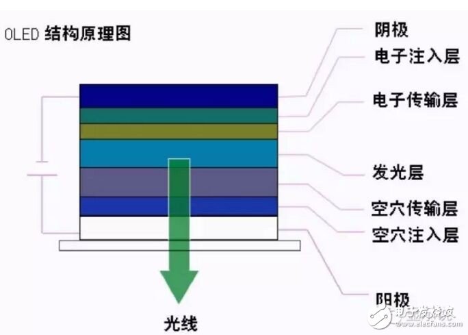
According to the working principle and materials used, the ultrasonic transducer has piezoelectric transducer, electrostatic transducer (capacitive transducer), magnetostrictive transducer, electromagnetic acoustic transducer, mechanical transducer and other types [1].