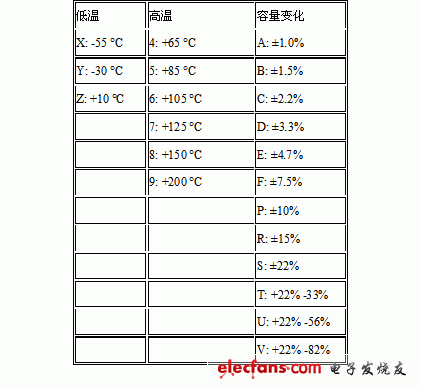
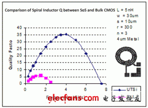
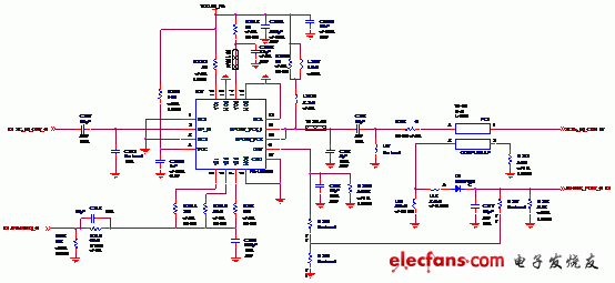
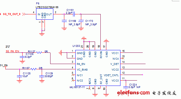
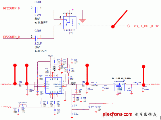
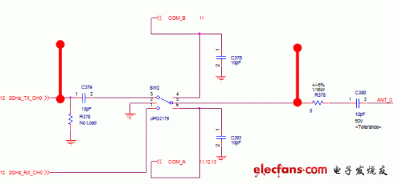
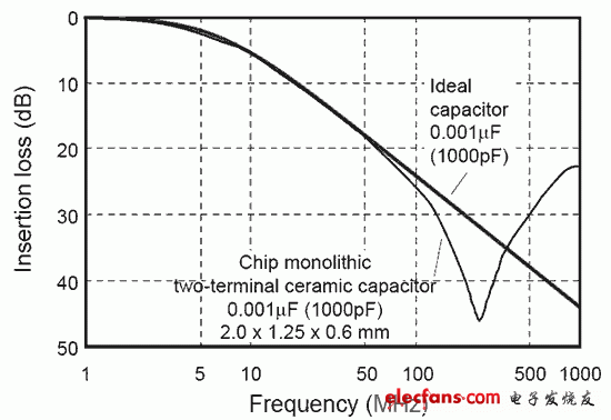
This document is a series of RF debugging experiences in the Wi-Fi product development process summarized by the first-line RF engineers of Sanghua Communication. It records and describes the process of encountering and solving problems in actual project development. This article refers to the address: http:// 1 Introduction This document summarizes some of the Radio Frequency debugging (hereafter called Debug) experience I have been working for for a year and a half, documenting the process I encountered and solved in actual project development. Now I want to use this document to share these experiences with you. If this document can help everyone's work, it will be my greatest honor. Personally, the Debug process uses the simplest basic knowledge. If you can have a deep understanding of RF basics (attention, it is extremely profound), I believe that all bugs will be easy to solve. Again, my documentation will cover the most straightforward Debugging techniques in the most accessible language. In this article, I try to avoid writing some empty theoretical knowledge, except for the contents of Chapter 2. The "Passive Devices at Microwave Frequency" section captures the "long story" that has not yet been completed - the general RF circuit design for Wi-Fi products (Second Edition). I believe that this document has more than one error. If it can be found by everyone, I hope that it can be proposed so that we can make progress together. 2 Passive devices at microwave frequencies In this chapter, we mainly talk about passive components at microwave frequencies. A simple problem: a 1K resistor has a resistance of 1K in DC and may be 1K in a 10MHz loop, but at 10GHz? Will its resistance be 1K? the answer is negative. At microwave frequencies, we need to look at passive components in another way. 2.1. Conductors at microwave frequencies The wire at the microwave frequency can exist in many ways, and can be a microstrip line, a strip line, a coaxial cable, a component pin, or the like. 2.1.1. Skin effect In the low frequency case, the current inside the wire is uniform, but at the microwave frequency, a strong magnetic field is generated inside the wire, which forces the edge of the electron guide to gather, so that the current flows only on the surface of the wire. This phenomenon is called the skin effect. The skin effect causes the resistance of the wire to increase. What happens? The attenuation is severe when the signal is transmitted along the conductor. 2.1.2. Linear inductance We know that a magnetic field is generated around a wire through which a current flows. If the current in the wire is an alternating current, the strength of the magnetic field changes with the change of current. Therefore, a current change is prevented at both ends of the wire. The voltage, this phenomenon is called self-inductance. That is to say, the wire at the microwave frequency exhibits the characteristics of an inductor, which is called a linear inductor. Maybe you will have a small linear inductance that can be ignored, but we will see in the following that as the frequency increases, linear inductance becomes more and more important. The concept of inductance is very important, because at the microwave frequency, any wire (or conductor) will exhibit certain inductance characteristics, even the resistor, the capacitor pin is no exception. 2.2. Resistance at microwave frequency Fundamentally, resistance is a characteristic that describes the resistance of a material to current flow. The relationship between resistance and current, voltage is given in Ohm's law. However, at the microwave frequency, we cannot use Ohm's law to simply describe the resistance. At this time, the characteristics of the resistor should have undergone great changes. 2.2.1. Equivalent circuit of resistance The equivalent circuit of the resistor is shown in Figure 2-1. Where R is the resistance of the resistor itself under DC conditions, L is the pin of the resistor, and C is different due to the structure of the resistor. It is easy to think that at the same frequency, the same resistor will exhibit different resistance values. Think about the design of Wi-Fi products in our country, almost no need to directly insert components (except large-capacity electrolytic capacitors), on the one hand to reduce the volume, on the other hand, it is more important reason, reduce the components The inductance caused by the pin. Figure 2-1 Equivalent circuit of the resistor Figure 2-2 qualitatively shows the relationship between the resistance of the resistor and the frequency. Figure 2-2 Resistance and frequency of the resistor We tried to analyze why resistors have such characteristics. When the frequency is 0 (corresponding to the DC signal), the resistance exhibited by the resistor is its own resistance; when the frequency is increased, the resistance exhibited by the resistor is its own resistance plus the inductance of the inductor; When the frequency is further increased, the resistance of the resistor itself plus the inductance of the inductor is already quite large, so the resistance exhibited by the resistor is the capacitive reactance of the capacitor in parallel, and the higher the frequency, the smaller the capacitive reactance. 2.3. Capacitance at microwave frequency In RF circuits, capacitors are a widely used component such as bypass capacitors, interstage coupling, resonant tanks, filters, and more. Like resistors, the capacitive reactance characteristics of capacitors at microwave frequencies can vary greatly. 2.3.1. Capacitor equivalent circuit We know that the material of the capacitor determines the characteristic parameters of the capacitor. The equivalent circuit of the capacitor is shown in Figure 2-3. C is the capacitance of the capacitor itself, Rp is the insulation resistance in parallel, Rs is the heat loss of the capacitor, and L is the inductance of the pin of the capacitor. Figure 2-3 equivalent circuit of the capacitor Regarding the capacitor, I am here to introduce a few parameters that people usually may not pay attention to when selecting materials. Figure 2-4 qualitatively shows the reactance characteristics of the capacitor at different frequencies. The vertical axis in the figure is the insertion loss (Insertion Loss), which is the loss due to the addition of capacitance. Figure 2-4 Reactance characteristics of capacitors at different frequencies Obviously, before the turning point, the capacitor shows the characteristics of the capacitor. After the turning, the capacitor exhibits the characteristics of the inductor. In general, a large-capacity capacitor exhibits more inductance characteristics than a small-capacity capacitor. Therefore, at a frequency of 250MHz, a 0.1uF bypass capacitor is not necessarily better than a 100pF capacitor. In other words, the classic formula of capacitive reactance It seems that when the frequency is constant, the larger the capacity of the capacitor, the smaller the capacitive reactance. But at the microwave rate, the conclusion is the opposite. At microwave frequency, a 0.1uF capacitor will exhibit greater impedance than a 100pF capacitor. This is why we have to design a power supply circuit with a large capacity electrolytic capacitor; small capacitors are connected in parallel at both ends. The capacity of the capacitor is used to eliminate high frequency noise signals. 2.3.2. Capacitance capacity and temperature characteristics When selecting materials in the CIS library, we will always find that the capacitance has a parameter of X7R or X5R, NPO, etc. I hereby search for relevant information, translate it and write it in this section. These parameters describe the dielectric material type, temperature characteristics, and error parameters used in the capacitor. Different values ​​also correspond to a range of capacitance capacities. Specifically, it is: X7R is commonly used for capacitors with a capacity of 3300pF~0.33uF. This type of capacitor is suitable for filtering, coupling, etc. The dielectric constant is relatively large. When the temperature changes from 0°C to 70°C, the capacitance change is ±15%. Y5P and Y5V are commonly used for capacitors with a capacity of 150pF~2nF. The temperature range is wide. With temperature changes, the capacitance varies from ±10% or +22%/-82%. For other coding and temperature characteristics, you can refer to Table 2-1. For example, X5R means that the normal operating temperature of the capacitor is -55 ° C ~ +85 ° C, the corresponding capacitance capacity changes ± 15%. Table 2-1 Temperature and capacity error codes for capacitors 2.4.1. Inductive equivalent circuit It is not difficult to imagine that there is a certain resistance in the wire itself, and there is a certain capacitance before the adjacent coil, so we get the equivalent circuit of the inductor shown in Figure 2-5. Where Rs is the resistance of the wire, L is the inductance of the inductor itself, and C is the equivalent capacitance. The inductance-frequency curve of the inductor is quite similar to the impedance-frequency curve of the resistor, which is directly related to their similar equivalent circuits. The reader can analyze the frequency characteristic curve of the inductor by himself. Figure 2-5 The equivalent circuit of the inductor 2.4.2. Q value of the inductor The ratio of the inductive reactance of the inductor to the series resistance Rs is called the Q value of the inductor, that is, Q=X/Rs is similar to the capacitor. The larger the Q value, the better the quality of the inductor. If the inductor is an ideal inductor, then the Q value should be infinite, but in reality there is no ideal inductor, so an inductor with an infinite Q value does not exist. At low frequencies, the Q of the inductor is very large, because at this time Rs is only the DC resistance of the wire, which is a small value. When the frequency increases, the inductance X of the inductor will become larger, so the Q value of the inductor will increase with the increase of frequency (the skin effect is not obvious at this time); however, when the frequency is increased to a certain extent At this time, the skin effect cannot be ignored. At this time, the series resistance Rs will become larger as the frequency increases, and the series capacitor C also starts to function, causing the Q value to decrease as the frequency increases. Figure 2-6 shows the Q-value vs. frequency of an inductor in a company. Figure 2-6 Curve of Q value and frequency of inductance of a company In order to maximize the Q value of the inductor, we can usually use the following methods when making the inductor: Use a larger diameter wire to reduce the DC resistance of the inductor; Pulling the coil of the inductor apart can reduce the distributed capacitance between the coils; Increase the permeability of the inductor, which is usually achieved with a magnetic core, such as a ferrite core. In fact, the manual production of inductors is a compulsory course for RF engineers, but this part of the content is more complicated. This article will not be discussed at this time. Interested readers can refer to relevant literature. 3 RF Debug experience sharing 3.1. A wireless AP 2.4GHz Chain0 has no output power During a test of a wireless AP (dual-frequency high-power 11n wireless AP), I suddenly heard a sound of cracking sound, and then saw a smoky smoke slowly rising from the board (unfortunately did not see the specific In which position), the surrounding area is quickly filled with unpleasant scorching odor, and the power on the VSA (Vector Signal Analyzer) drops below 0 dBm. Anyone with a little experience can draw a conclusion: "There is something burned." There is no output power. It is conceivable that a certain device of the Tx circuit must be damaged, but which one is it? First, the visual method is used (the so-called visual method is to directly observe the appearance of the component with the eyes to see if there is a crack or burnt mark), and the result is not seen. Then use the “point test methodâ€. At this time, you may ask: “What is the point measurement method?†The point measurement method is to directly detect the signal state of the point to be measured by using a probe or a probe, which is often used for time domain signal detection. Such as an oscilloscope, but because Wi-Fi products have a higher operating frequency, signal detection is generally performed in the frequency domain, and point detection is rarely used for detection. Practice has proved that the point test method is a fast and effective means to determine the RF problem. Say the starting point measurement method, I have to talk about the production of simple probes. Take an SMA Cable (as shown in Figure 3-1), remove the SMA connector at one end (do not remove both ends), and strip the shield of 1~2cm in length to expose the core. In this way, a common SMA Cable turned around and upgraded to a spot probe, which became a detection tool and became a good assistant for RF engineers. 3.2. Excessive output power Phenomenon: The output power is super large, and the constellation diagram is blurred and cannot be demodulated. This is a slightly more complicated issue. We know that Atheros's solution will have the control part of the output power, that is, let Target Power and the actual power value be consistent. How is this achieved? We took out the 2.4GHz PA part of the AP96 circuit for research, as shown in Figure 3-2. Figure 3-2 2.4GHz PA circuit In Figure 3-2, U27 and its peripheral circuits form a power amplifier that is sent to subsequent circuits via C208 and R263. PC1 in the figure is a printed directional coupler. The voltages of the 3 and 4 pins increase with the output power. L18, L19, D1, C217 and R248 form a half-wave rectification circuit and will be oriented. The voltage sensed by the coupler becomes a DC signal and is sent to Transceiver for detection, which is the AR9223_PDET_0 network. In this way, Transceiver can always know the current output power, and the relationship between power and voltage value is established in the process of Calibrate. After the board passes Calibrate and loads the EEPROM, we use the ART to perform the Continue Tx. At this time, the board will signal according to the Target Power we set. Transceiver will increase its output power until the corresponding voltage value recorded in the Calibrate process ( AR9223_PDET_0) is consistent. At this time, we returned to the beginning of the question "output power is super large, the constellation map is blurred, can not be demodulated", what is going on? It must be that Transceiver can't get the correct voltage value, so it can only increase its output power until the PA output power is saturated. Check L19, L18, D1, C217, R248 and find that D1 has been opened, replace it with a new diode and return to normal. It should be pointed out here that the use of directional couplers for output power control is a unique method of Atheros. This method has not been seen in Broadcom and Ralink. In addition, the PA itself usually has a built-in power detection unit and is output through a pin, usually V_DET. 3.3. A wireless network card has a severe static fever Phenomenon: After a wireless network card is powered on, no operation is performed. The four PAs emit a lot of heat. The surface temperature of the PA is very high and it is very hot. The first judgment is that PAs are not really "static", they are working secretly! So how do you verify it? Take the Demo board of PA (SKY65137-11) and use Power Supply to observe the current consumed. After power-on, it is found that the current consumed is almost zero, and there is no heat generation, which is different from the case of the wireless network card. Studying the SKY65137-11's Datasheet, a key pin PA_EN caught my attention. This pin is the PA enable pin. In the case of power-on, this pin is pulled up to 3.3V, and it is found that the current consumed by 5V is sharply increased, and a large amount of heat is emitted, and the surface temperature of the PA rises immediately. Disconnect PA_EN from 3.3V, and the current consumed by 5V will drop. At this time, touch the PA_EN pin by hand and find that the current consumed by 5V is beating, which means that the weak electrical signal sensed by the human body is enough to make the PA " The Enable state also states that PA_EN is a very sensitive pin and that a very weak signal is sufficient to trigger. Analyze the SKY65137-11 unit circuit of the wireless network card, as shown in Figure 3-3 (excluding Level Shift). Figure 3-3 SKY65137-11 unit circuit It is easy to find that the PA_EN pin of SKY65137-11 is directly connected to the control pin of AR9220 through a Level Shift circuit, so that the weak disturbance of the AR9220 control pin can trigger the PA, so it will cause the PA to be heated under static conditions. . Solution: Use a 10K resistor at the PA_EN pin to pull down the ground, so that the PA is normally off. Through the above method, the problem of heat generation of PA is solved. 3.4. A wireless network card Calibrate is not allowed Phenomenon: After the wireless network card passes Calibrate, the actual output power is inconsistent with Target Power. First, check to make sure that it is not a problem with Cable Loss and ART. The RF part of the wireless network card is designed by us. There are too many uncertain factors. There is no in-depth analysis here. As discussed in 3.2, Atheros' solution achieves stable output power by detecting the voltage value corresponding to the output power of the PA; in the static case, if the PA has no output power, the corresponding voltage value is zero. Through detection, it is found that the V-Detect output by the SKY65135-21 (2.4GHz PA) in static state is not zero, but a voltage value of a few volts, which may be caused by the problem of the PA itself, and it is for this reason that The problem of the Calibrate of the wireless network card is not allowed. We all know the unidirectional conduction characteristics of the diode. In order to prevent the 2.4 GHz and 5 GHz bands of the wireless network card from interacting with each other in the Calibrate process, they can be separated by a diode. In the subsequent version of the wireless network card, we have adopted this method, which can solve the problem of accurate Calibrate. 3.5. A wireless AP has no output signal Phenomenon: ART runs normally, observes with VSA, and has no output signal. Recalling the content explained in 3.1, we mentioned the point measurement method. Personally, the point measurement method is the fastest way to solve such a problem. In the case of using ART for Continue Tx, the probe is used to detect the Transceiver output in turn. PA input, PA output, low-pass filter output, T/R Switch input and T/R Switch output. In general, it is enough to detect these points. According to the above method, we sequentially detect each point of the Tx loop (using 2.4GHz link 0 as an example), as shown in Figure 3-4. Figure 3-4 2.4GHz 0 link detection point During the actual detection process, it was found that there is a signal at the input end of the T/R Switch, that is, there is a normal RF signal at C379, but there is no signal at the output of the T/R Switch. Check the Datasheet of the T/R Switch uPG2179 and find that The control signal at this time does not match the expected. For details, please refer to the reference design of uPG2179 Datasheet and AR9280 (Transceiver for this project).
ZGAR MINI
ZGAR electronic cigarette uses high-tech R&D, food grade disposable pod device and high-quality raw material. All package designs are Original IP. Our designer team is from Hong Kong. We have very high requirements for product quality, flavors taste and packaging design. The E-liquid is imported, materials are food grade, and assembly plant is medical-grade dust-free workshops.
From production to packaging, the whole system of tracking, efficient and orderly process, achieving daily efficient output. We pay attention to the details of each process control. The first class dust-free production workshop has passed the GMP food and drug production standard certification, ensuring quality and safety. We choose the products with a traceability system, which can not only effectively track and trace all kinds of data, but also ensure good product quality.
We offer best price, high quality Vape Device, E-Cigarette Vape Pen, Disposable Device Vape,Vape Pen Atomizer, Electronic cigarette to all over the world.
Much Better Vaping Experience!
ZGAR Vape Pen,Disposable Device Vape Pen,UK ZGAR MINI Wholesale,ZGAR MINI Disposable E-Cigarette OEM Vape Pen,ODM/OEM electronic cigarette,ZGAR Mini Device Zgar International (M) SDN BHD , https://www.szvape-pods.com
In practical high-frequency applications, such as the induction coil of a radio, in order to reduce the signal attenuation caused by the skin effect, it is common to use multiple strands of wires to be wound side by side without using a single wire.
We usually use the skin depth to describe the skin effect. Skin depth is a function of frequency and the wire itself, and we won't discuss it in depth here. 

![]()
