Figure 1 Beam-mass block structure Sensitive structure of the sensor In order to solve the above problems, this paper takes "small deformation-large stress" as the design idea, and seeks suitable sensor sensitive structure, so that the sensor has a large structural rigidity, while the varistor is still at a large sensitive stress, The sensitivity of the sensor is improved, and three kinds of piezoresistive acceleration sensors with beam film structure, double-bridge structure and multi-beam structure are designed. The beam film structure (Fig. 3) is an improvement on the traditional cantilever beam structure, which improves the natural frequency of the sensor and reduces the lateral cross interference of the sensor. At the same time, the smaller film structure thickness can reduce the influence of the natural frequency rise on the sensitivity of the sensor. The double-bridge structure (Fig. 4) and the composite multi-beam structure (Fig. 5) are based on the traditional double-bridge structure. The former introduces stress-concentrated holes to reduce the sensitivity of the sensor while reducing the loss of sensitivity of the sensitive structure. The introduction of short sensitive beams, while increasing the natural frequency of the sensor, uses the strain amplification of the structure to provide higher measurement sensitivity for the sensor. Micromachining of sensor chips 1) Wet etching and lobe compensation. 2) Ion implantation. 3) ICP etching. 4) Silicon-glass anodic bonding. 1) Cleaning the silicon wafer and thermally oxidizing on both sides to obtain SiO2 layer. 2) The varistor of the silicon wafer is doped with boron in the P-region to the required concentration. 3) Boron ion implantation in the metal contact region to form a P+ region 4) Sputtering metal, front side lithography, forming aluminum leads. 5) Front protection, back ICP etching to form mass block active damping gap. 6) Depositing Si3N4 layer by low pressure chemical vapor deposition, while depositing SiO2 layer to reduce film stress and form KOH etching mask layer. 7) Backside lithography, etching the backside SiO2 and Si3N4 to form a mask layer of KOH etching, the reticle provides the convex angle compensation pattern of the moving mass, the back side KOH anisotropic etching, forming the active mass, and the front ICP release Composite multi-beam structure. 8) The silicon wafer is bonded to the glass sheet having the anti-adsorption electrode by an anodic bonding technique, and then diced to complete the process to obtain a sensor chip. A Home Projector that supports WiFi connection, usually an Android system, can connect to the same WiFi to realize screen sharing. In addition to multimedia functions, you can also watch videos, download software and play games online. Mainly focusing on high-quality goods, the projection screen is clear and true, suitable for home, office, teaching, and entertainment wifi mini home projector,wifi protable home projector,bluetooth mini projector,HD mini projector Shenzhen Happybate Trading Co.,LTD , https://www.szhappybateprojectors.com
When the sensor is subjected to acceleration, the mass is displaced in proportion to the acceleration under the action of the inertial force, causing the support beam to undergo bending deformation and stress. Due to the piezoresistive effect of silicon, the resistance of the varistor changes under stress, and then the voltage proportional to the acceleration is output through the Wheatstone bridge to realize the conversion of the acceleration signal to the electrical signal, as shown in Fig. 2. 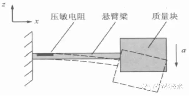

Figure 2 Piezoresistive sensor operation process In the process of processing the sensor chip, the ion-implantation process is usually used to make four equivalent varistor in the most sensitive area of ​​the sensor stress to improve the measurement sensitivity of the sensor. Then, the varistor is connected by a metal lead on the chip to a Wheatstone bridge, and is excited by an external constant voltage source or a constant current source. When the sensor is operating, the Wheatstone bridge can effectively convert the varistor into a voltage signal, and the voltage output of the piezoresistive sensor is linear with the acceleration input. 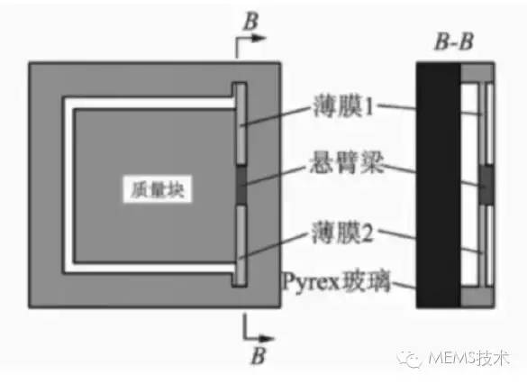 Figure 3 Schematic diagram of the beam film structure
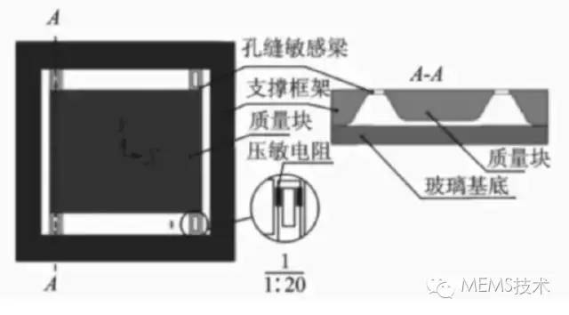
Figure 4 Schematic diagram of the double-bridge structure 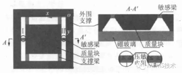
Figure 5 Schematic diagram of composite multi-beam structure 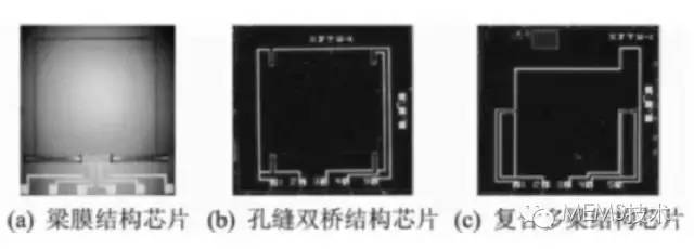
Figure 6 Processed sensor chip The MEMS accelerometer in this paper uses processing technology that can be integrated with the IC process. Its low cost, miniaturization and mass production potential enable MEMS sensors to be monitored wirelessly in future intelligent mechanical equipment fault information. A large number of applications have been obtained to replace the more expensive piezoelectric acceleration sensors currently in use. At the same time, "small deformation - large stress" is an effective design idea in the design of high frequency response and high sensitivity acceleration sensors. The small-thickness membrane structure introduced by the beam membrane structure, the stress-concentrated pore joint introduced by the double-bridge sensor of the slit and the short sensitive beam introduced by the composite multi-beam structure all improve the performance of the sensor to some extent.
As the data source for fault information monitoring and diagnosis, the sensor directly determines the accuracy of subsequent fault diagnosis for the picking accuracy of engineering equipment working parameters, and is the key device for mechanical fault information monitoring. With the trend of wireless monitoring systems entering industrial applications and the intelligent development of manufacturing equipment, the piezoelectric accelerometers currently used cannot gradually meet the actual needs of the industry due to cost and volume; therefore, they will be miniaturized and large-scale. The production of potential MEMS sensors for mechanical fault information monitoring can provide necessary device support for the integrated and intelligent development of manufacturing equipment. Combining the advantages and disadvantages of various types of sensors and the performance requirements of vibration detection sensors for mechanical manufacturing equipment fault detection, this paper introduces the working principle and structure of micro-vibration acceleration sensor with three different structures of piezoresistive MEMS accelerometers. The micro-machining process, based on the constraint relationship between the natural frequency of the sensor and the measurement sensitivity, proposes a sensitive structure design method of “small deformation-large stressâ€, and formulates the sensor chip fabrication process according to the designed structural characteristics and micro-machining process capability. Acceleration Sensor Operation The piezoresistive sensor uses the piezoresistive effect of the material to convert the physical quantity into an electrical quantity to achieve signal measurement. At present, the piezoresistive accelerometer mostly adopts the "beam-mass block" structure as shown in Fig. 1, and mainly includes three basic components of a mass block, a support beam and a varistor.