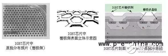
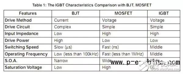
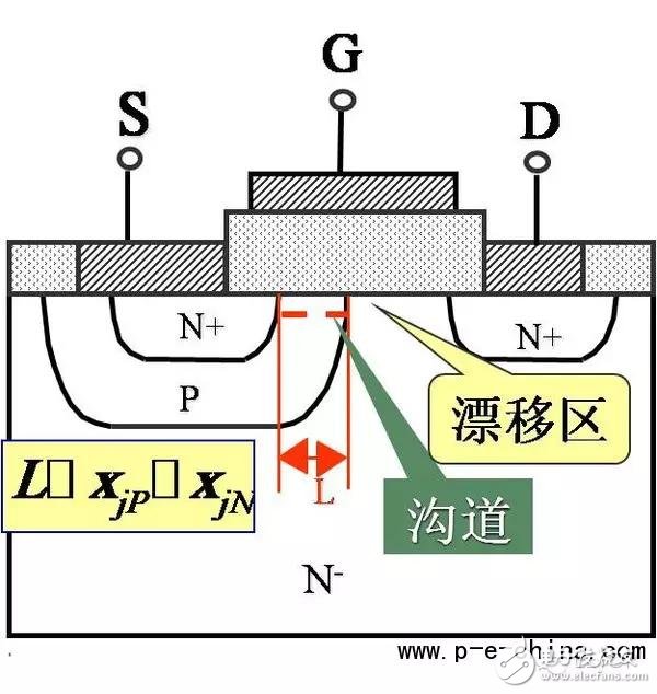
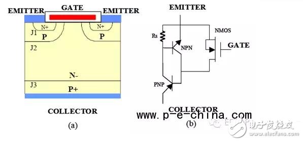
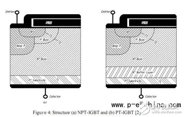
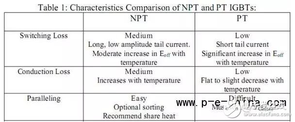
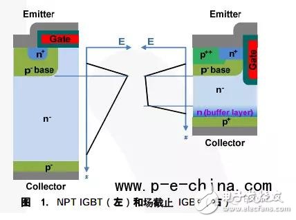
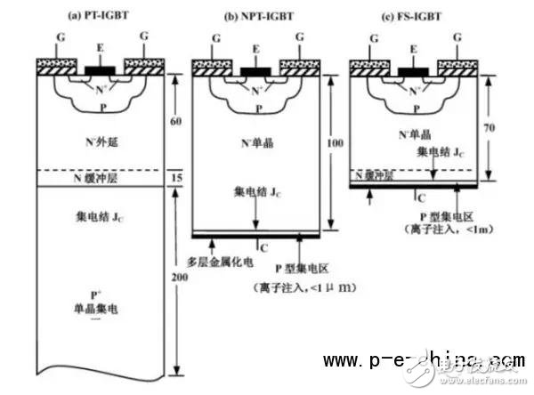
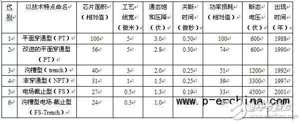
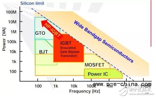
The IGBT is a voltage-controlled power transistor that you can think of as a high-power version of a CMOS tube. The characteristics are high switching frequency, the main applications of the family such as inverter air conditioner, induction cooker, microwave oven, as well as the active pfc and UPS of the computer power supply. Industrial applications are mainly used for various motor drives. From a functional point of view, IGBT is a circuit switch used on high voltages with voltages on the order of tens to hundreds of volts and currents ranging from tens to hundreds of amps. The discovery of electricity is a revolution in human history. The kinetic energy generated by it is constantly being released every day. The demand for electricity is no less than the oxygen of the human world. If there is no electricity, human civilization will be explored in the dark. However, the most important component in power electronics is the IGBT. Without IGBT, there will be no convenient life for high-speed rail. When it comes to IGBTs, people in semiconductor manufacturing think that they are not a discrete device (Power Disceret). However, like 28nm/16nm integrated circuit manufacturing, he is the key support project of the national “02 special projectâ€. This is the most advanced technology in power electronics, and has completely replaced the traditional Power mosFET. Small to home appliances, large aircraft, ships, transportation, power grids and other strategic industries, known as the "CPU" in the power electronics industry, for a long time, the product (including chips) is still monopolized in a handful of IDM ( FairChild, Infineon, and TOSHIBA) ranked second in the country's 16 major technological breakthroughs during the 12th Five-Year Plan period (referred to as “02 Special Projectâ€). The IGBT is called an Insulated Gate Bipolar Transistor, so it is a BJT transistor with MOS Gate. Strange, is it MOSFET or BJT? In fact, it is not all. Not a circle, he is a combination of MOSFET and BJT. I mentioned their advantages and disadvantages when talking about MOSFETs and BJTs. MOSFETs are mainly single-carrier (multi-sub) conductive, while BJT is two-carrier conductive, so the driving current of BJT is larger than MOSFET. However, the control stage gate of the MOSFET is controlled by the field effect inversion without additional control terminal power loss. Therefore, the IGBT combines the advantages of MOSFET and BJT, and has the gate voltage control transistor of the MOSFET (high input impedance), and utilizes the double carrier of BJT to achieve high current (low conduction voltage drop). (Voltage-Controlled Bipolar Device). In order to achieve the perfect requirements of small driving power and reduced saturation voltage, it is widely used in converter systems such as AC motors, inverters, switching power supplies, lighting circuits, traction drives and other fields above 600V. 2, the traditional power MOSFET In order to understand the IGBT, I will first talk about the structure of the Power MOSFET. The so-called power MOS is to withstand high power, in other words, high voltage, high current. We combine the general low-voltage MOSFET to explain how to change the structure to achieve high voltage and high current. 1) High voltage: If the general MOSFET has a high voltage of Drain, it will easily lead to breakdown of the device. The general breakdown channel is the other three ends of the device (S/G/B), so to solve the high voltage problem, the three must be blocked. end. The Gate end can only rely on the field oxygen pad under the Gate to isolate the drain-to-drain distance (Field-Plate), while the Bulk-side PN junction breakdown can only reduce the concentration on both sides of the PN junction, and the most annoying is to the Source end, it is A long drift region is required as a drain series resistor divider so that the voltage drops across the drift region. 2) High current: The channel length of a general MOSFET is determined by Poly CD, and the channel of the power MOSFET is controlled by the difference of the junction depth of the two diffusions. Therefore, as long as the process is stable, it can be made small and is not affected by light. The accuracy of the engraving. The current of the device depends on W/L, so if you want to get a large current, you only need to increase W. Therefore, the above Power MOSFET is also called LDMOS (Lateral Double diffusion MOS). Although such a device can achieve high power requirements, it still has its inherent disadvantages. Since its source, gate, and drain are all on the surface, the drain and source need to be pulled long, which wastes chip area. And because the device is on the surface, the complexity is increased and isolation is required if the device is to be connected in parallel. So later developed VDMOS (VerTIcal DMOS), the drain is uniformly placed on the back of the Wafer, so that the drift region length of the drain and source can be controlled by the backside thinning, and such a structure is more conducive to the between the tubes. The parallel structure achieves high power. However, the LDMOS structure is still used in the BCD process in order to be compatible with CMOS. Let me talk about the development and evolution of VDMOS. The earliest VDMOS is to directly put the LDMOS Drain on the back through the back thinning, Implant, metal evaporation (as shown below), he is the legendary Planar VDMOS, it The challenge compared to traditional LDMOS is the back side process. But its advantage is that the front process is compatible with traditional CMOS processes, so it is still alive. However, this structure has the disadvantage that its channel is transverse to the surface and the area utilization is still not high enough. Later, in order to overcome the shortcomings of Planar DMOS, VMOS and UMOS structures were developed. Their approach was to dig a groove in the Wafer surface and change the channel of the tube from the original Planar to the verTIcal along the wall. It was a clever idea. But a pie always matches a trap (IC manufacturing is always trade-off). The inherent disadvantage of this structure is that the slot is too deep and the electric field is concentrated, resulting in breakdown, and the process is difficult and costly. The bottom of the groove must be absolutely routing, otherwise it is easy to break down or generate stress lattice defects. However, its advantage is that the number of crystal saturation is much larger than the original, so more transistors can be connected in parallel, which is more suitable for low voltage and high current applicaTIon. There is also a classic thing called CoolMOS, everyone learn google yourself. He should be considered the highest voltage of Power MOS, which can reach 1000V. The Power MOSFET is described above, and the IGBT is essentially a field effect transistor. It is very close to the Power MOSFET in terms of structure. It adds a P+ layer to the drain electrode on the back side. We call it InjecTIon Layer (the origin of the name, etc.) Said below). . The Power MOSFET described above is basically a traditional MOSFET. It is still a single carrier (multiple sub-conductor), so we have not yet exerted its ultimate performance. So later developed a new structure, how can we inject the hole from the drain side in addition to the MOSFET's own electrons when the Power MOSFET is turned on? So naturally, a P+ injection layer is introduced at the leaky end (this is the origin of the name), and a P+/N-drift PN junction is added from the structural leak, but he is positively biased, so it is not The influence of conduction increases the hole injection effect, so its characteristics are similar to those of BJT. There are two kinds of carriers participating in conduction. So the original source becomes Emitter, and Drain becomes Collector. From the above structure and the equivalent circuit diagram on the right, it has two equivalent BJTs linked back to back. It is actually a PNPN Thyristor. This thing is not what we deliberately do, but the structure is generated. I wrote an article about Latch-up (http://ic-garden.cn/?p=511) five months ago. The most terrible thing about this structure is the Latch-up. The key to controlling Latch-up is to control Rs, as long as α1+α2 is satisfied. In addition, such a structural advantage is to improve the current drive capability, but the disadvantage is that when the device is turned off, the channel is quickly turned off without multiple sub-currents, but the Collector (Drain) side continues to have minority hole injection. Therefore, the current of the entire device needs to be slowly turned off (tailing current), which affects the turn-off time and operating frequency of the device. This is a taboo for switching devices, so a structure is added to add an N+buffer layer between P+ and N-drift. This layer is used to allow the device to inject holes from the Collector when it is turned off. It is quickly compounded in the N+ buffer layer to increase the turn-off frequency. We call this structure PT-IGBT (Punch Through type), and the original NPT-IGBT without N+buffer. In general, NPT-IGBT is higher than Vce(sat) of PT-IGBT, mainly because NPT is positive temperature coefficient (P+ substrate is thinner and less hole injection), and PT is negative temperature coefficient (because P substrate is thicker) Therefore, the hole injection is more caused by the triode base region modulation effect, and Vce (sat) determines the switch loss, so if the same Vce (sat) is required, the NPT must increase the thickness of the drift, so Ron has increased. The process front of the IGBT is not worse than the standard LDMOS of the BCD, but the back is more difficult: 1) Back thinning: generally required 6~8mil, this thickness is difficult to grind and easy to chip. 2) Back injection: all grind to 6~8mil, and also hit High current P+ implant 》E14's dose, it is easy to be fragmented, and there must be special equipment dedicate. Even the fourth generation has two Hi-current injections, which is the limit. 3) Back cleaning: This general SEZ is fine. 4) Back metallization: This can only be done by metal evaporation process, Ti/Ni/Ag standard process. 5) Back Alloy: The main consideration is that the wafer is too thin and easy to warp the pieces. 1) Field cutoff FS-IGBT: No matter whether PT or NPT structure can not meet the requirements of infinite high power, to achieve high power, it is necessary to lower Vce (sat), that is, reduce Ron. Therefore, it is necessary to reduce the thickness of the N-drift, but this N-drift thickness is again constrained by the electric field of the off-state (too thin to easily pass through). Therefore, if you want to reduce the thickness of the drift, you must let the cut-off electric field drop before the channel. Therefore, it is necessary to introduce an N+ field stop layer (FS) between the P+ injection layer and the N-drift. When the IGBT is in the off state, the electric field rapidly drops to 0 in the cut-off layer to achieve the purpose of termination, so we can Further reducing the N-drift thickness reduces Ron and Vce. Moreover, this structure is very similar to the N+ buffer structure, so it also has the effect of PT-IGBT to suppress the tailing current in the off state to increase the closing speed. The question is, what is the difference between this and the N+ buffer of the PT-IGBT? In fact, the production process is different. The PT-IGBT is made with two layers of EPI, which is the first layer of ~10um N+ buffer on the P+ substrate, and then the second layer ~100um of N-Drift. This cost is very high! In contrast, the FS-IGBT is based on the NPT-IGBT directly on the back side of the high-concentration N+ cut-off layer, the cost is relatively low, but the challenge is how to achieve no fragmentation under thinner thickness. 2) Anode short circuit (SA: Shorted-Anode): Its structure is that the N+ collector is intermittently inserted into the P+ collector, so that the N+ collector directly contacts the field stop layer and serves as the cathode of the PN diode, while P+ continues to do its FS. The collector of the IGBT, which has enhanced current characteristics and changes the cost structure, since there is no need to co-package the anti-parallel diodes. Experiments have shown that it can increase the saturation current and reduce the saturation pressure drop (~12%). IGBT You can use it as a MOSFET in series with a PiN diode, or as a wide base PNP driven by a MOSFET (DarlinGTOn structure), the former can be used to understand its characteristics, the latter is his principle. It seems that the IV curve of a MOSFET has been shifted backwards ("0.7V), because the channel turn-on current must satisfy the drift region current and the drift region resistance multiplied by more than 0.7V to make the P+ substrate and N-drift The PN junction is conducting, so that it can work, otherwise the channel can not work. Finally, let's blow the bulls. Everyone often hears the first generation of IGBTs until the sixth generation of IGBTs. What do these mean? 1) The first generation: he is the prototype of IGBT, the simplest schematic structure diagram, so he must increase N-drift to improve the withstand voltage, so the on-resistance and turn-off power consumption are relatively high, so there is no popularization. use. 2) The second generation: PT-IGBT, since the depletion layer cannot penetrate the N+ buffer layer, the electric field in the base region is strengthened in a trapezoidal distribution, so the chip thickness can be reduced to reduce power consumption. This is mainly the product BSM150GB120DN1 of Siemens Company from 1990 to 1995 ("DN1" is the meaning of the first generation). It has advantages mainly at 600V (similar to GTR characteristics), and when it reaches 1200V, it has a problem of high thickness, high cost, and low reliability (poor concentration and uniformity of thickness). 3) The third generation: NPT-IGBT, no longer uses epitaxial technology, but uses ion implantation technology to generate P+ collector (transparent collector technology), which can accurately control the junction depth and control the emission efficiency as low as possible. Fast carrier extraction speed to reduce turn-off loss, can maintain the original carrier lifetime of the base region without affecting steady-state power consumption, and has a positive temperature coefficient characteristic, so the technology is mature in steady state loss and shutdown A good compromise has been made between losses, so it is widely used. On behalf of the company is still the first batch of products that Siemens adopts FZ (zone melting method) instead of extension, representing products BSM200GB120DN2, VCE"1200V, Vce(sat)=2.1V. 4) The fourth generation: Trench-IGBT, the biggest improvement is the Trench structure, the channel runs from the surface to the vertical surface, so the PIN effect of the base region is enhanced, and the carrier concentration near the gate is increased, thereby improving The conductance modulation effect reduces the on-resistance, and since the channel is not on the surface, the JFET effect is eliminated, so the gate density increase is not limited, and the third-generation collector continues to use the third-generation collector P+. The implant technology also incorporates the second generation of PT technology as a field stop layer, effective extra high withstand voltage capability. The need to use dual injection technology is more difficult. This time is the era of Infineon. Infineon's thinning technology ranks first in the world. Its thickness can be reduced to 120um~140um at 1200V (200um for NPT-IGBT), and even reduced to 70um at 600V. 5) The fifth generation: FS-IGBT and the sixth generation FS-Trench, the fifth and sixth generation products are recombination of various technical measures after the IGBT has experienced the above four technical improvement practices. The fifth-generation IGBT is a combination of the fourth generation of products "transparent collector technology" and "electric field suspension technology". The sixth generation of products improved the trench gate structure on the basis of the fifth generation and appeared in a new look. At present, China's overall energy utilization efficiency is about 33%, which is about 10% lower than that of developed countries. At present, China's energy conservation work faces great pressure. In the field of new energy, China has become the largest country in the production of solar cells, and the cumulative installed capacity of wind power has doubled for four consecutive years, which means that China's new energy market has huge business opportunities. Whether it is solar cells, wind power or new energy vehicles, its system applications need to convert DC power to AC power. The components that undertake this task are called inverters. The core component of the inverter is IGBT (Insulated Gate Bipolar Transistor), which is also one of the most expensive components. In foreign countries, IGBT technology and products are constantly updated, and China does not currently have the ability to mass produce IGBTs. It is the IGBT technology for high-speed rail produced by Zhuhai CSR and CNR, as well as China Resources Microelectronics (who wants to acquire Fairchild), and Huahong Hongli seems to have it. Now the state supports 8-inch IGBT technology. ShenZhen Haofa Metal Precision Parts Technology Co., Ltd. , https://www.haofametals.com