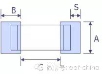
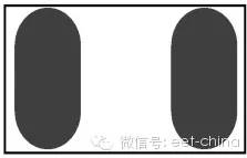
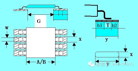
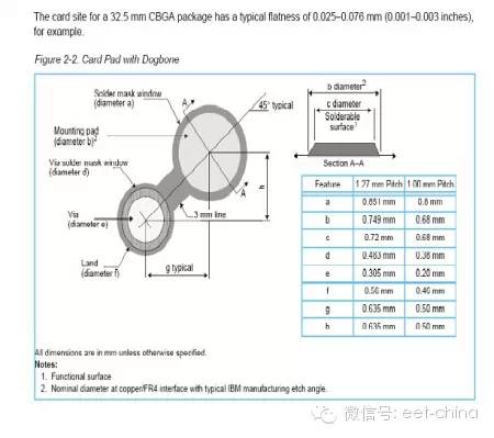
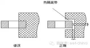
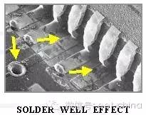
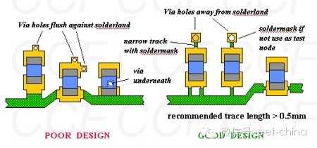
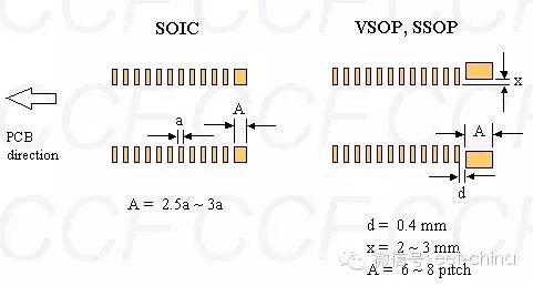
The component pad design of the PCB is a key point, and the quality of the final product lies in the quality of the solder joint. Therefore, whether the pad design is scientific and reasonable is crucial. For the same component, any symmetrical pad (such as chip resistor, capacitor, SOIC, QFP, etc.) should be designed to maintain its full symmetry, that is, the shape and size of the pad pattern should be exactly the same. In order to ensure that the solder melts, the surface tension (also called the wetting force) of all the solder joints on the component can be balanced (ie, the resultant force is zero) to facilitate the formation of the ideal solder joint. The following classifications refer to the pad design requirements for different types of components: First, the chip component pad design should master the following key elements symmetry: the pads on both ends must be symmetrical to ensure the balance of the surface tension of the molten solder; Dimensional components 0603, 0402, 0201, etc., the imbalance of the surface tension of the solder at both ends, it is easy to cause the defects of the components to form a "tombstoning". Pad pitch: ensure the proper overlap size of the component terminals or pins and pads; the remaining dimensions of the pads: the remaining dimensions after bonding must ensure that the solder joints can form a meniscus; pad width: should be with the component ends Or the width of the pins is basically the same. A : pad width B : pad length G : pad pitch S : pad remaining size In actual production, the most common 0402 component pad design is unreasonable, resulting in more defects. Here, we give you a preferred pad design for 0402 components. This solution has better performance in production and has a very low defect rate. . 0402 preferred pad parameters and land pattern: A = 0.7-0.71B = 0.38G = 0.52S = 0.14 Both ends of the pad can be designed to be semi-circular, and the solder joints after soldering are relatively full. Second, SOP and QFP design principles: 1, the pad center distance is equal to the pin center distance; 2, the general principle of a single pin pad design Y = T + b1 + b2 = 1.5 ~ 2mm (b1 = 0.3 ~ 1.0mm b2 =0.3~0.7mm)X=1~1.2W3, the inner distance of the two rows of pads is calculated by the following formula (unit: mm) G=FK type: G—the distance between the two rows of pads, F—component housing Package size, K-factor, generally 0.25mm, The SOP includes the QFP pad design. Note the two parameters b1 and b2 in the second section above. Good solder joints can be seen in the figure below. In this figure, the toe of the solder joint previously referred to as the solder joint, the qualified solder joint must contain both parts, and it is indispensable. The strength of the point is also guaranteed by these two parts, especially the heel area. In some cases of poor design, either b2 is too short, or b1 is too short, resulting in the inability to form qualified solder joints. Third, the BGA pad design principle 1, the center of each pad on the PCB coincides with the corresponding ball center of the bottom of the BGA; 2, the PCB pad pattern is a solid circle, the via hole can not be processed on the pad 3, the width of the wire connected to the pad should be the same, generally 0.15mm~0.2mm; 4, the size of the solder mask is 0.1mm~0.15mm larger than the pad size; 5. The via hole near the pad is metallized It must be blocked with solder resist, the height should not exceed the height of the pad; 6. The screen pattern is processed at the four corners of the BGA device, and the line width of the screen pattern is 0.2mm~0.25mm. The pad shape of a BGA device is circular, and typically the PBGA pad diameter should be 20% smaller than the solder ball diameter. The through hole next to the pad must be soldered during the board to prevent short circuit or solder joint caused by solder loss. The BGA pad pitch should be designed according to the metric system. Since the component manual will give the metric and inch sizes, the components are actually produced in the metric system. The design of the pads in the inch system will cause installation deviation. The PBGA mentioned above is a plastic package. The material of the lead PBGA solder ball is 63Sn37Pb, which is consistent with the composition of the lead solder, and melts at the same time as the solder during the soldering process to form a solder joint. The lead-free PBGA solder ball is SAC307 or SAC305, which is similar to the commonly used lead-free solder and melts during soldering to form solder joints. But there is also a BGA, the package is ceramic, called CBGA, CBGA solder ball is a high temperature solder, its melting point is much higher than the common solder, in the welding, CBGA solder ball is not melted, therefore, CBGA The pad design is not the same as the PBGA pad design. Specific design parameters can refer to the following figure: 4. Thermal isolation of the pad When the pin of the SMD device is connected to the large-area tube foil, it should be thermally isolated. Otherwise, the solder will be defective due to uneven heat at both ends of the device. Fifth, the setting of the via hole of the reflow soldering process 1. The diameter of the general via hole is not less than 0.75mm; 2. Except for SOIC, QFP, PLCC and other devices, the through hole cannot be guided under other components; 3. The via hole cannot be designed on the solder surface. The position between the two pads; 4, it is not allowed to directly use the via hole as the pad of the BGA device; 5. There should be a thin wire coated with a solder mask between the via hole and the pad. The length of the thin wire should be greater than 0.5mm; the width should be greater than 0.4mm. It is absolutely necessary to avoid the placement of the via holes in the surface mount pads. The via holes should be placed within 0.635 mm from the surface mount pads. The vias should be connected through a small length of wire and the solder drain channel should be blocked by solder resist. Defects such as "slices" or "insufficient solder". Sixth, the plug-in component pad design 1, the hole pitch is 5.08mm or more, the pad diameter should not be less than 3mm; 2, the hole pitch is 2.54mm, the minimum pad diameter should not be less than 1.7mm; 3, the circuit board The pad pitch connecting the voltage of 220V should be no less than 3mm; 4. The diameter of the pad with a current exceeding 0.5A (including 0.5A) should be greater than or equal to 4mm; 5. The pad should be as large as possible. Generally, the solder joint has a pad diameter of at least 2 mm. When the plug-in component pad aperture design adopts the wave soldering process, the component jack aperture is generally 0.1 mm-0.3 mm larger than the lead wire diameter, and the diameter of the pad should be larger than 3 times of the aperture. The mounting hole distance of the resistor and diode should be designed as standard series 7.5mm, 10mm, 12.5mm, 15mm. The mounting hole distance of the electrolytic capacitor should be consistent with the component pin pitch, and the mounting hole distance of the triode should be 2.54mm. 7. When using the wave soldering process, when the pad design of the chip component is wave soldered to the chip component, attention should be paid to the occurrence of "shadow effect (missing) and 'bridge" (short circuit). For CHIP components, The axial direction of the component is perpendicular to the direction of transmission of the PCB. The small component should be in front of the large component, and the spacing should be greater than 2.5mm. Several points of the pad design should be used in the wave soldering process. 1. Elliptical soldering should be used for high-density wiring. Disk pattern to reduce the welding; 2, in order to reduce the shadow effect and improve the welding quality, the wave pattern of the wave soldering is designed for SOT, tantalum capacitor, the length of the pad outside the extension component, and the length direction should be better than the normal design. The disk extends outward by 0.3mm; 3. For SOP, to prevent bridging, widen the two outermost pads of the SOP to absorb excess solder; or set up a process pad (also known as a thief pad). The process pad is an empty pad that absorbs excess solder and is positioned behind the last pad in the transfer direction. Eight, the design of silk screen characters 1, the general situation needs to mark the silk screen graphics of the components in the silk screen layer, silk screen graphics including silk screen symbols, component number, polarity and IC first foot mark, high density narrow spacing can be used Simplify the symbol, in special cases, the bit number of the component can be omitted; 2. The polarity of the component should be marked according to the actual installation position and the installation direction; 3. For the integrated circuit with two or four sides leading to the foot, use Symbols (such as small squares, small circles, small dots) mark the position of the first pin, the size of the symbol should be proportional to the real object; 4, BGA devices are best marked with a matrix of Arabic numerals and English letters The position of the first foot; 5, for the connector type component, the mounting direction and the position of the 1st foot should be marked. 6. All the above markings should be outside the component mounting frame to avoid covering after welding and it is not convenient to check. 7, silk screen characters should be clear, the size is the same, the direction is as neat and tidy, easy to find; 8, the lines, symbols, etc. in the characters must not be pressed against the pad, so as not to cause poor soldering.
We are professional audio manufacturing company that makes a variety of speaker with bluetooth, including bluetooth portable speaker, bluetooth speakers outdoor, small speaker bluetooth, light bluetooth speakers, waterproof speakers etc.
With full turnkey service from product design to delivery, and every step in between.
From sophisticated custom audio systems to 'off-the-shelf' speaker drivers, iTopnoo has been saving our customers time, effort, and money.
To constantly offer clients more innovative products and better services is our consistent pursuit.
Best Portable Speakers,customizable bluetooth speaker, Custom jbl speakers, speaker wholesalers TOPNOTCH INTERNATIONAL GROUP LIMITED , https://www.itopnoobluetoothes.com