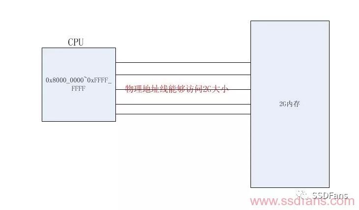
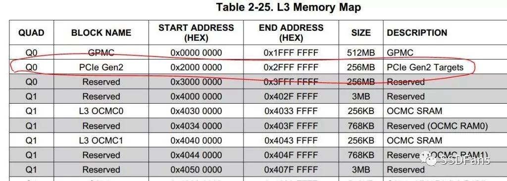
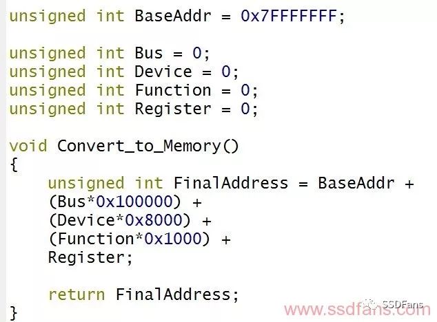
I. Overview CPU access to peripheral registers and memory addressing mode; How does the CPU access the PCIe configuration space; The CPU can access the configuration space through registers, why do you need to map the PCIe configuration space; How to scan the PCIe tree and assign ID to PCIe; How to map the pcie domain address to the memory domain address space. Through this article, questions 1, 2, and 3 will be answered. 2. Unified addressing versus independent addressing CPU addressing is a way to establish a link between program instructions and physical address lines. There is a special address set inside the CPU. The addressing process is determined by the CPU architecture. The reference schematic diagram is shown in Figure 1 (only the schematic diagram, explain one This kind of logical structure does not represent the actual circuit). The address space 0x8000_0000~0xFFFF_FFFF has been specified when the CPU is addressed as the address line connected to the memory in the figure. How to connect the memory to the CPU needs to refer to the datasheet of the CPU. When the CPU program instruction initiates access to the physical address of 0x8000_0000, It is equivalent to accessing the first address of the 2G memory in the figure. figure 1 The memory is addressed and located through the CPU address bus, and then data is read and written through the CPU data bus. The number of bits of the address bus of the CPU is determined when the CPU is designed, so the address range that a CPU can address is certain, and the memory needs to occupy the addressing space of the CPU, and the memory and the CPU are directly connected by a bus. IO refers to various peripherals connected to the CPU. There are two ways for the CPU to access various external devices: one is similar to the way of accessing memory, that is, the peripheral registers are read and written as memory addresses. Access the memory mode to operate peripheral registers. At this time, IO and memory are unified addressing, and IO addresses and memory addresses are in the same address space. This addressing method is called IO and memory unified addressing. Another addressing method is separate and independent addressing of the IO address and the memory address. This addressing method is called independent addressing. At this time, the CPU access to the peripheral registers needs to access the peripheral registers through the specific instructions of the CPU. The address directly accesses the peripheral registers. Common ARM, PowerPc, and MIPS architectures all use unified addressing, and X86 architectures use independent addressing. 3. Access to PCIe configuration space 256bytes The PCI bus specifies bus transactions that access the configuration space and use ID numbers for addressing. The PCI device ID number consists of Bus Number, Device Number and Function Number. The bus number is determined when the HOST host bridge traverses the PCI bus tree. On a PCI bus tree, the bus number is determined by the system software. Usually, the PCI bus number directly connected to the HOST host bridge is 0. The system software uses DFS (Depth -First Search) The algorithm scans all PCI buses on the PCI bus tree and numbers them sequentially. The device number of a PCI bus is determined by the connection relationship between the IDSEL signal of the PCI device and the PCI bus address line, and the function number is related to the specific design of the PCI device. A PCIe system has a maximum of 256 buses, each bus can be connected to a maximum of 32 devices, and each PCIe device has a maximum of 8 functional devices. In the HOST host bridge in the XX processor, the registers related to the PCIE device configuration are composed of CFG_ADDR, CFG_DATA, etc. The system software uses CFG_ADDR (the CFG_ADDR register structure is shown in Figure 2) and CFG_DATA register to access the configuration space of the PCIe device. These registers are all addressed by the same address (all memory registers are addressed using memory mapping). When the processor accesses the PCIe configuration space, it first needs to set the bus number, device number, function number, and register offset corresponding to the PCIe device in the CFG_ADD register, and then enable the Enable bit, and then when the processor reads and writes to CFG_DATA , The HOST host bridge converts this memory read and write access into a PCIe configuration read and write request, and sends it to the PCIe bus. If the Enable bit is not enabled, then the CPU access to the register is an ordinary IO access, and the HOST cannot be converted into a bus request access. When accessing the PCIe configuration space, configure the TLP request according to the PCIe bus standard, and CFG_DATA is the read data Or the data to be written. figure 2 31 bit: Enable bit, when it is 1, read and write CFG_DATA can be converted into PCIe bus configuration request. 30~24 bits: reserved. 23~16 bits: bus number, up to 256. 15~11 digits: device number, max=32. 10~8 digits: function number, max=8. 7~2 bits: register offset, maximum access register=64 addresses, where one address is DW, then the PCIe configuration space size for capable access is 64*4=256Byte, so access to PCIe configuration space is aligned with 4 bytes Visited. Many readers here may have such questions. Since the CPU can directly access the configuration space through the register, why does the mapping of the configuration space in the storage domain address appear? A detailed answer is given below. The method of accessing PCIe configuration space registers needs to be traced back to the original PCI specification. In order to initiate the PCI bus configuration cycle, Intel (Intel is the leader of PCIe, the latest PCIe specification is always its first attempt) implemented PCI specification uses CF8h and CFCh in IO space as index and data registers, respectively. This method Can access 255 bytes configuration registers of all PCI devices. Intel Chipsets still supports this method of accessing PCI configuration space. The PCIe specification expands the configuration space to 4K bytes on the basis of the PCI specification. As for why it is expanded to 4K, please refer to the PCIe specification for details. These methods of configuring CFG_ADDR and CFG_DATA registers can still access the first 255 bytes of the configuration space of all PCIe devices, but This method cannot access the remaining (255B~4K) configuration space. How to do it? A PCIe configuration space access method outside Intel. Intel Chipset maps the configuration space to the memory address space, and the PCIe configuration space can be accessed like read/write memory within the mapping range. This kind of mapping is done by the North Bridge chip, but the mapping method of different chips is also different. At present, I checked the datasheet of the ARM chip, and it is indeed this way. The PCIe specification adds more configuration registers for each PCIe device with a space of 4K. Although the CFG_ADDR and CFG_DATA register methods can still access the lower 255 bytes, another method must be provided to access the remaining (255B~4K) range register. Intel's solution is to use the reserved 256MB memory address space, and any access to this memory will initiate a PCIe configuration cycle. Since the 4K configuration space is directly mapped to memory, the PCIe specification must ensure that the configuration space of all PCIe devices occupies different memory addresses. According to the PCIe specification, it supports up to 256 buses, and each bus supports up to 32 PCIe devices. Each device supports up to 8 functions, that is to say: the maximum occupied memory is: 256 * 32 * 8 * 4K = 256MB. Figure 3 is a partial map of ARM Cortex-A9 datasheet memory address allocation. The 256M memory space occupied by the PCIe configuration space will shield the DRAM from using this memory area, and these addresses have been solidified by the CPU when it leaves the factory. image 3 Fourth, the impact of the memory mapping of the PCIe configuration space on the 32bit system Because PCIe configuration space occupies 256M memory space, and the occupied space is not available to DRAM, this means that 256M space disappears in system memory, which is more obvious in 32bit systems. For example, in 32 bit winxp (the author still uses the XP system for the computer, the computer has been used for seven or eight years), theoretically the memory that can be accessed is 4G, if the 4G space is occupied by DRAM, due to the existence of PCIe, The part of the memory space occupied by PCIe is unavailable to the OS. It disappears inexplicably up to 256M of memory. In fact, there are other peripheral registers that need to be mapped to the memory. If it is independent addressing, there is no register to occupy the memory. Therefore, the maximum actual DRAM space that can be accessed in the XP system is 3.2G. This situation does not exist for 64-bit CPU addressing. At present, the address should not be used up. Readers need to pay attention to that the CPU has 32 and 64-bit addressing modes, and the operating system also has 32 and 64 bits. In Linux system Mainly reflected in the library file. Some CPUs do not directly specify the address range of the PCIe configuration space and need to read the value BaseAddr of a certain register. This value refers to the base address of the PCIe configuration register mapped in the memory area. When accessing the PCIe device configuration space, you need to manually calculate the address for accessing the PCIe configuration space. The calculation and distribution are as follows: SIZE_PER_FUNC = 4K = 1000h SIZE_PER_DEVICE = 4K * 8 = 8000h SIZE_PER_BUS = 4K *8* 32 = 100000h The calculation formula for accessing the offset register whose bus number is busNo, device number is DevNo, and function number is funcNo is: Memory Address = BaseAddr+ busNo * SIZE_PER_BUS+ devNo * SIZE_PER_DEVICE+ funcNo * SIZE_PER_FUNC+ offset To access the PCIe configuration space, it is necessary to convert the bus number, device number, function number, and register offset into a memory address. The conversion function is shown in Figure 2. Figure 4 Questions 4 and 5 will be explained in the next article, because the author is limited. If there are errors, we hope readers will give valuable comments. Medium Voltage SWA Armored Cable Medium Voltage SWA armored cable is a type of Power Cable that is designed to transmit electricity at medium voltage levels. The cable is constructed with a steel wire armoring layer that provides mechanical protection and helps prevent damage from external factors such as impact, moisture, and rodents. The armored layer also provides additional protection against electrical faults, making it a popular choice for underground and overhead installations. Medium Voltage SWA Armored Cable,Medium Voltage Underground Cable,Steel Wire Armoured Power Cable,Outdoor Armored Cable Ruitian Cable CO.,LTD. , https://www.rtlinecable.com


The cable is typically made up of a copper or aluminum conductor, which is insulated with a cross-linked polyethylene material. The XLPE insulation provides excellent electrical properties, such as high dielectric strength and low capacitance, which help reduce power losses and improve efficiency.
Medium Voltage SWA armored cable is commonly used in a variety of applications, including power distribution, industrial plants, and renewable energy projects. The cable is available in different sizes and voltage ratings, ranging from 8.7 kV to 15 kV, and can be customized to meet specific project requirements.