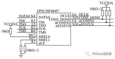
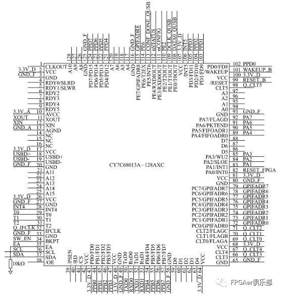
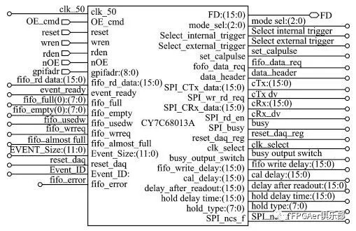
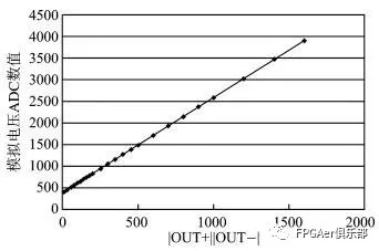
When designing a PC-based data acquisition system, engineers all believe that in order to obtain better performance, they all need to use the PCI bus. In fact, this is not the case. With the continuous development of USB communication technology, the transmission speed and reliability of the USB bus are gradually improving. For the wide range of USB2.0 applications, its fastest speed can reach 480 Mb/s. Even if some of these interrupts or protocols occupy part of the bandwidth, speeds higher than 80 Mb/s are easy to achieve. The theoretical speed under the USB3.0 protocol can reach about 10 times that of USB2.0. In addition, compared to the PCI card, the USB interface is more convenient for system development and upgrades. QuickUSB[1] is a high-speed USB module for USB2.0 developed based on CY7C68013A[2]. Bitwise provides this module with a low-level program embedded in EEPROM, and at the same time provides the corresponding LabVIEW and C language API low-level program on the PC side, which provides great convenience for the development of the system. The system [3] designed in this paper is based on this principle. 1 hardware circuit design The core hardware of the system is FPGA, ADS803E, CY7C68013A and Bitwise's EEPROM embedded with the underlying program. Figure 1 is the FPGA configuration circuit. CY7C68013A can configure FPGA through PS mode without the need for other downloaders. The FPGA model selected by the system is EP2C50F484. In order to download in PS mode, you need to set MSEL0=1, MSEL1=0, and MSEL2=0 respectively. Note that the configuration port needs to add a pull-up resistor to ensure its normal operation. Figure 1 FPGA configuration circuit The system chooses ADS803E as the ADC conversion circuit. The conversion speed of ADS803E can reach 5 MHz, and its pins are compatible with the same type of 10 MHz ADS804 and 20 MHz ADS805. Figure 2 is the system ADC conversion circuit. The input signal of ADS803E must be followed by an operational amplifier first, in order to control the input signal within its measurement range. The measuring range of ADS803E can be realized by changing the value of resistance R1 and R2 in the figure, and its measuring range is 0~2×R1+R2R1. The output of ADS803E will be valid after 6 clocks, which means that its digital output has a delay of 6 clocks for analog input. At the same time, in order to reduce the power consumption of the system, when ADC conversion is not needed, the clock of ADS803E can be stopped through FPGA. Figure 2 ADC conversion circuit Figure 3 Schematic diagram of CY7C68013A The schematic design of CY7C68013A is shown in Figure 3. Including 9 address lines (GPIF_ADR0~8), 16 data lines (PPB0~7, PPD0~7), and corresponding control lines. FPGA and CY7C68013A connection software interface is shown as in Fig. 4. With the corresponding read and write control timing designed and written by CY7C68013A, it can communicate with the PC, and at the same time operate the ADC according to the obtained control commands, and read the obtained data from the FIFO and transfer it to the PC. Figure 4 FPGA and CY7C68013A connection software interface 2 Control software design The process of the data acquisition system is abbreviated-editor's note. All the initial configuration of the system is written in a TXT file. When the program starts to run, it will read the file according to the set path and initialize all configuration information. The software uses the method of reading PC environment variables to enhance the portability of the software system. When you need to transfer the software system from one PC to another, you only need to change the definition of environment variables. FPGA receives data and control commands from the PC through CY7C68013A, converts them into memory read and write, A/D conversion, front-end electronics control and other commands, and finally transmits the measured data to the PC. 3 Test results The test result is shown as in Fig. 5, uses the direct current power source as the test source to carry on the performance test to the data acquisition system. Test OUT+ and OUT- for the changes of 0~1.2 V and -1.2~0 V, and then get the ADC conversion result from the PC. The abscissa in the figure is the sum of |OUT+| and |OUT-|, and the ordinate is the ADC value corresponding to the analog voltage. By fitting the data in the figure, the linear relationship between the analog signal and the digital signal y=357.144+2.223x is obtained. This means that every mV voltage corresponds to a digital output of 2.2, which can also be expressed as an analog voltage corresponding to 0.45 mV per digital value. The intercept of the line on the Y axis is called the base value, which is generally 300 to 400 ADC counts. Figure 5 Linearity test of the data acquisition system 4 Conclusion The QuickUSB-based data acquisition system can realize rapid data acquisition and storage, and has obvious advantages in terms of volume and power consumption. The system has been applied to many experiments [6] (such as the PEBS experiment), and good test results have been achieved. Hybrid Split Phase Solar Inverter Shenzhen Jiesai Electric Co.,Ltd , https://www.gootuenergy.com


