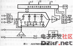
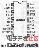
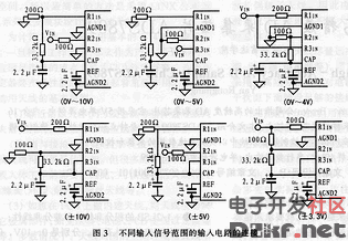
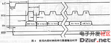
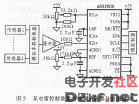
Chinese introduction of high precision AD acquisition chip ADS7809 The ADS7809 is a high precision AD acquisition chip from Burr-Brown. It is powered by a single 5V supply and contains 16-bit successive approximation registers with high sampling accuracy and low power consumption. This paper introduces the main features and functional structure of the ADS7809. An example of how to apply the ADS7809 to a mine control equipment system for high-speed data acquisition and control. To maximize the combat effectiveness of weaponry, The automation of modern weapons and equipment is getting higher and higher, which requires the weapon equipment to continuously detect various operating parameters during its operation, so that the control system is always in the best running state. In the process of some mine control equipment developed by us, in order to collect the data of each sensor in real time, in order to effectively control the impact precision of the whole weapon equipment, the design has adopted the AD conversion chip AD67**ADS7809 with 16-bit precision. The experimental results show that under the same working conditions, the stability of ADS7809 is higher than that of AD676. The following mainly introduces the performance and characteristics of the high-precision AD conversion chip ADS7809 produced by Burr-Brown. 1 Main features of the ADS7809 The ADS7809 has the following features: a capacitor-based successive approximation register type analog-to-digital converter with 16-bit sample-and-hold; â— 100kHz sampling rate, the signal to noise ratio of the input at 20kHz is 83dB; â—Integral nonlinearity and differential nonlinearity of +1/2LSB; â— 6 selectable input ranges, 0~10V, 0~5V, 0~4V, ±10V, ±5V and ±3.3V; â— On-chip with +2.5V reference source, can also use external reference source; â— The chip has its own clock, and the sampled data is output through serial. Data can be output either by internal clock or by external clock. â—Powered by a single 5V power supply, the maximum power consumption is less than 100mW; â— Available in a 20-pin plastic DIP package or SIOC package. Operating temperature range is -25 ° C ~ +85 ° C. 2 internal structure and pin description Figure 1 is a block diagram of the ADS7809, and Figure 2 is its pin package diagram. The description of each signal pin is as follows: R1IN, R2IN, R3IN: Three analog input selections for different input ranges; Figure 3 shows the input circuits for different input ranges. CAP: Reference snubber capacitor. Connect a 2.2μF tantalum capacitor to ground; REF: Reference input/output. Connect a 2.2μF tantalum capacitor to ground; AGND1, AGND2: analog ground; SB/BTC: Select the data output format. Select the offset code output when high level, and select two-complement output when low level; EXT/INT: Select external/internal clock to send data. Select internal clock transmission when low level; SYNC: Synchronous output. If EXT/INT is high, the SYNC output will output a SYNC sync pulse when CS is low and when the rising edge of the R/C pin comes, or when R/C is high and the falling edge of the CS pin comes. External DCLK; SCLK: Clock input or output, depending on the state of the EXT/INT pin. The output data is synchronized by the clock; SDA: serial data output; TAG: Cascade input for external clock mode. If EXT/INT is high, the signal input to this pin is output from the SDA pin after a delay of 16 pulses; R/C: Read/convert pulse input. If CS is low, the R/C pin will control the sample/hold circuit mid-on hold on its falling edge and initiate an AD conversion. If EXT/INT is low, the result of the last AD sampling is started. If EXT/INT is high, then when CS is low and the rising edge of R/C pin is high or R/C is high and the CS pin is falling. Edge, send a sync pulse on the SYNC pin to initiate the transmission of data; CS: Chip select signal pin. Logically "or" internally with the R/C signal; BUSY: Busy status output. Low when the conversion starts, and remains "low" until the end of the conversion and the data is latched into the output shift register; PWRD: Power down input. When it is high, the chip enters the power-down state to further reduce power consumption; VANA: analog + V power supply input; VDIG: Digital +5V power supply input DGND: Digital ground. 3 data serial output timing Figure 4 shows the timing of data serial output using the internal clock. Since the data output and the AD conversion use the same clock source, after the R/C pulse, the output data is the value of the last AD sample, not the result of the current AD conversion, which should be noted. 4 Typical applications Figure 5 is a block diagram showing the circuit composition of a data acquisition part of a mine control device. The signals from the various sensors are switched by the analog switch and sent to the buffer follower, which reduces the output impedance of the signal source to ensure high acquisition accuracy. The ADS7809 is connected to a ±5V input form to generate AD conversion and data output from the internal clock. The microcontroller controls the sampling time of the ADS7809 through the R/C signal. The eight-channel patrol detection takes about 100 μs at a time, and the mine control device achieves good results in the implementation. Building Visual Intercom Column Customised Building Visual Intercom Columns,Stainless steel building visual intercom column,Building intercom access control system Shenzhen Jingtu Cabinet Network Equipment Co., LTD , https://www.jingtujigui.com