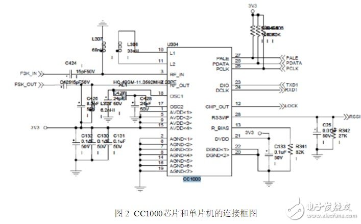
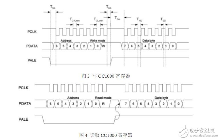
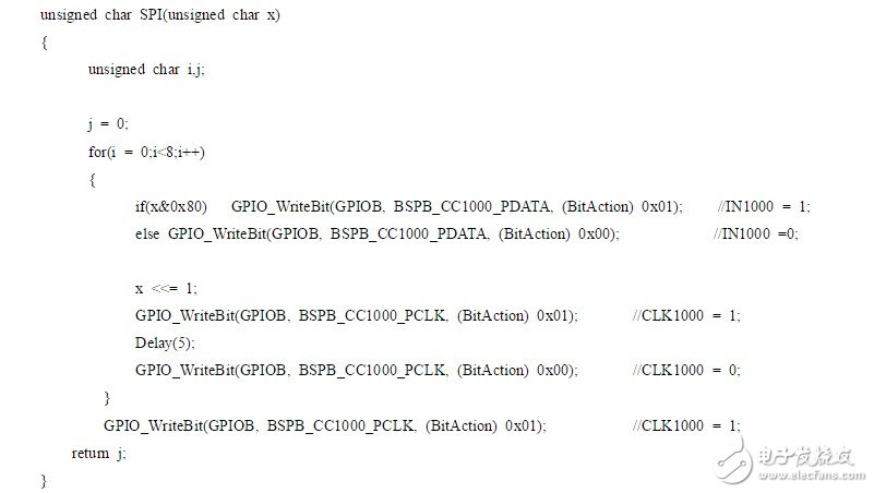
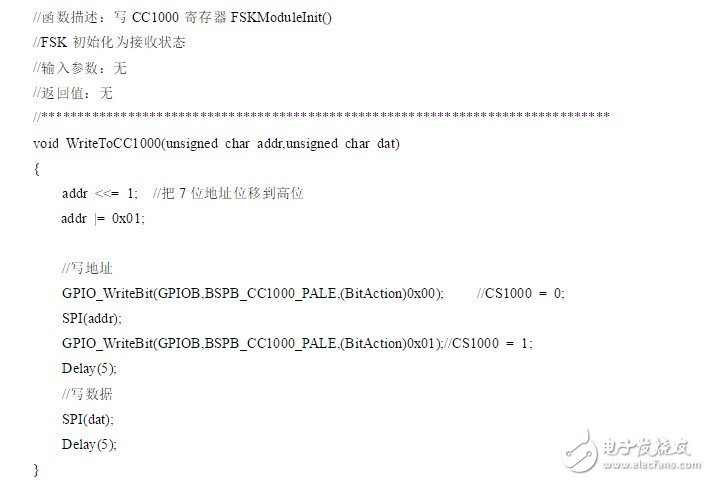
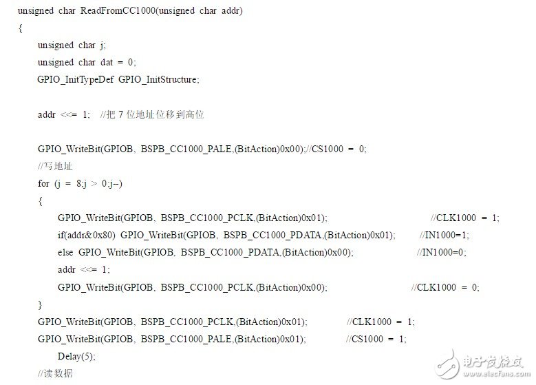
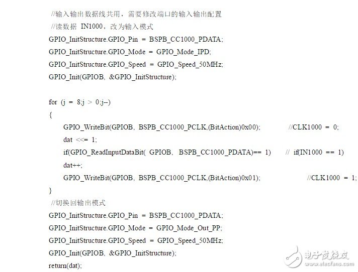
This article is mainly about the introduction of CC1000, and focuses on the CC1000 programming based on FSK modulation chip. CC1000 is an ideal UHF monolithic transceiver communication chip manufactured in 0.35μm CMOS process based on Chipcon's SmartRF technology. Its operating frequency band is 315, 868 and 915MHz, but CC1000 can be easily programmed to work in the range of 300-1000MHz. It has low voltage (2.3~3.6V), extremely low power consumption, programmable output power (-20~10dBm), high sensitivity (generally -109dBm), small size (TSSOP-28 package), integrated bit synchronizer Features. Its FSK data transmission can reach 72.8Kbps, with 250Hz step length programmable frequency capability, suitable for frequency hopping protocol; the main operating parameters can be programmed and changed through the serial bus interface, and it is very flexible to use. Circuit configuration In receiving mode, CC1000 can be regarded as a traditional superheterodyne receiver. The radio frequency (RF) input signal is amplified by the low noise amplifier (LNA) and then flipped into the mixer, where the intermediate frequency (IF) signal is generated through the mixer. In the intermediate frequency processing stage, the signal is amplified and filtered before being sent to the demodulator. The optional RSSI signal and IF signal can also be generated on the pin RSSI/IF by mixing. After demodulation, CC1000 outputs the demodulated digital signal from pin DIO, and the synchronization of the demodulated signal is completed by the clock signal provided by PCLK on the chip. In the transmission mode, the signal output by the voltage controlled oscillator (VCO) is directly sent to the power amplifier (PA). The RF output is controlled by the data added to the DIO pin, which is called Frequency Shift Keying (FSK). This internal T/R switching circuit makes the antenna connection and matching design easier. The local oscillator signal generated by the frequency synthesizer is sent to the power amplifier in the receiving state. The frequency synthesizer is composed of a crystal oscillator (XOSC), a phase detector (PD), a charging pulse, a VCO, and a frequency divider (/R and /N). The external crystal must be connected to the XOSC pin. Only the external inductor needs to be connected to the VCO Connected. Circuit connection of CC1000 The following is the connection block diagram and circuit diagram of the CC1000 chip and the microcontroller: Specific pin function introduction: The microcontroller controls the CC1000 to change different modes through the three serial configuration ports PDATA, PCLK and PALE. DIO and DCLK are the data signal interfaces between the CC100 and the MCU. The MCU sends data to the CC1000 chip through DIO, and sends the CC1000 chip to the CC1000 through DCLK. MCU data. The microcontroller can monitor the frequency lock status from the pin CHP_OUT (LOCK). CC100 outputs and receives signals to the antenna through RF_IN and RF_OUT. MCU read and write CC1000 register programming CC1000 can be programmed through simple three serial interfaces PDATA, PCLK and PALE. CC1000 mainly has 36 8-bit configuration registers, each of which is addressed by a 7-bit address. The read/write bit initiates a read or write operation. A complete configuration of CC1000 requires 29 data frames, each with 16 bits (7 address bits, 1 read/write bit and 8 data bits). The PCLK frequency determines the time required for the complete configuration. At 10MHz PCLK frequency, the time required to complete the entire configuration is less than 60µs. Only one frame needs to be transmitted when setting in the low-potential mode, and the time required is less than µ2s. All registers are readable. In each write cycle, 16-bit bytes are sent to the PDATA channel, and the 7 most important bits (A6:0) in each data frame are the address bits. A6 is the MSB (the most significant bit), which is sent first. The next bit to be sent is the read/write bit (high level write, low level read). During the transfer address and read/write bit period, PALE (program address latch enable) must remain low, and then transmit 8 The data bit (D7:0) is shown in Figure 3. This is the end of the introduction about the CC1000 programming based on the FSK modulation chip. If there are any deficiencies, please correct me. earphones headphones headsets earphones headphones headsets Shenzhen Linx Technology Co., Ltd. , https://www.linxheadphone.com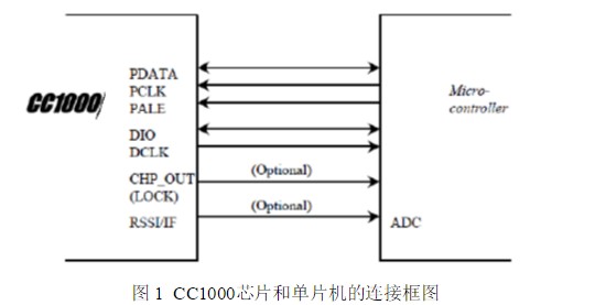


Related reading recommendations: based on low-power RF transceiver CC1000 to achieve wireless headset data transmission